
Semiconductor
Samsung is developing Z-NAND-O, Z-NAND-T, and Z-NAND-I for AI infra


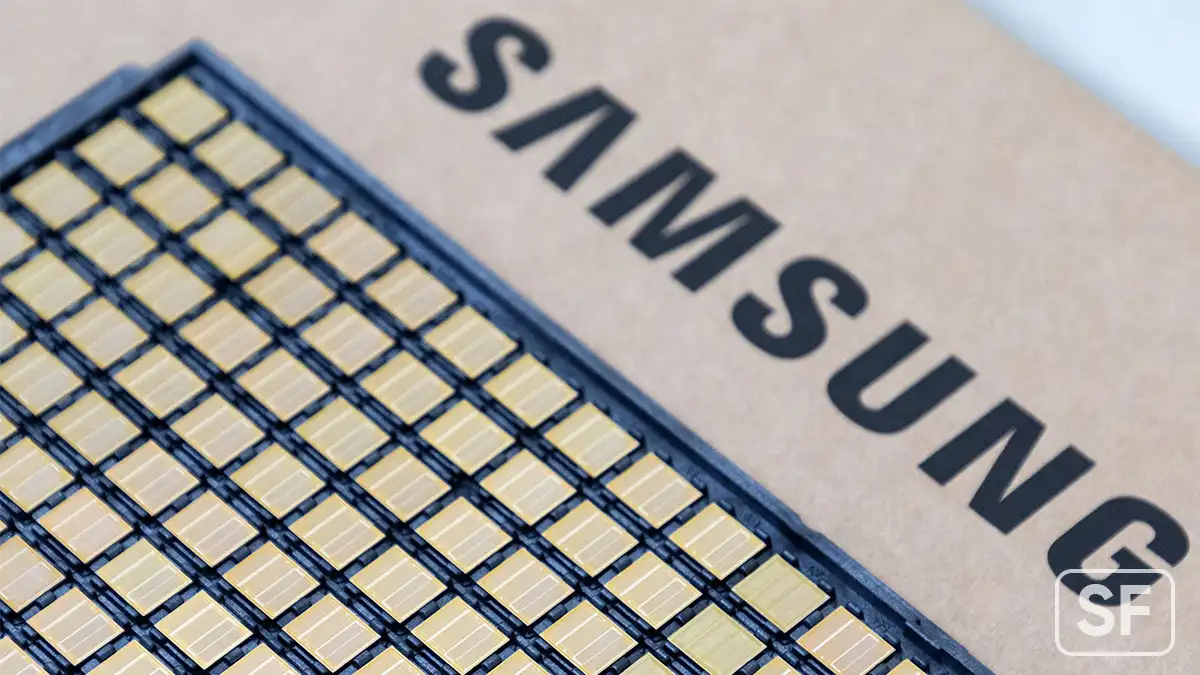
Samsung is developing three specialized versions of its next-generation Z-NAND memory technology to meet the growing demands of AI, with each variant targeting a different performance requirement.
According to ZDNet, Samsung is in the early stages of developing Z-NAND-O, Z-NAND-T, and Z-NAND-I. The company showcased a mockup of Z-NAND-O at a US memory industry event in August, offering an early glimpse of its next-gen memory strategy.
Z-NAND-O is designed for on-device AI
Z-NAND-O uses Through-Silicon Via (TSV) technology to stack NAND chips vertically in four or eight layers. It aims to improve data transfer speeds and power efficiency, two important factors for AI processing on mobile and other connected devices.
Z-NAND-T focuses on throughput and bandwidth
Z-NAND-T focuses on throughput and bandwidth, targeting high-performance AI data centers that need to move large amounts of data efficiently.
Z-NAND-I prioritizes input/output operations per second
Z-NAND-I prioritizes input/output operations per second (IOPS), measuring how many individual read and write operations memory can handle.

Meanwhile, Samsung has yet to officially announce the complete lineup or disclose specifications and launch timelines. The three-way approach suggests the company wants to tailor NAND tech to specific AI workloads instead of relying on a single design.
Notably, SK Hynix is also developing its AI-NAND Family, comprising AIN P for performance, AIN D for storage density, and AIN B for bandwidth.
As AI infrastructure expands, customized NAND could become increasingly important alongside conventional memory and storage.





Reports from credible news platforms suggest that Samsung plans to invest a massive $9.15 billion in the chip segment across Vietnam and South Korea.
Behind a massive $9.15 billion outlay across its various affiliates, Samsung is making a calculated move: doubling down on high-value domestic R&D while offloading labour-intensive backend processes across Vietnam and Korea.
At the heart of this push is a $4.09 billion investment from Samsung Electronics into a massive memory chip testing facility at the Yen Binh Industrial Park in Thai Nguyen, northern Vietnam.
Designed to handle final DRAM and NAND flash testing for silicon originally packaged at Cheonan, the site will act as a major pressure valve for Korean domestic operations starting in late 2027.
This move frees up critical floor space at home for bleeding-edge high-bandwidth memory (HBM) lines, a pivot Samsung desperately needs as AI server demands surge.
Meanwhile, Samsung Electro-Mechanics is pouring 6.78 trillion won into flip-chip ball grid array (FC-BGA) substrate capacity, splitting the funds between Korea’s Sejong and Vietnam.
The real test won’t be building the cleanrooms; it will be whether Vietnam can build a robust local supplier ecosystem around them, or remain just a high-tech assembly line.

Semiconductor
Samsung, SK Hynix and TSMC join Applied Materials’ $5 billion Semiconductor R&D hub to accelerate chip development

Applied Materials is officially opening its massive $5 billion EPIC Center in Sunnyvale, California, creating an unprecedented physical crossroads, with Samsung and SK Hynix signing on as founding partners alongside TSMC, Intel, and Micron.
According to Yonhap, Samsung, SK Hynix, TSMC, Micron, and Intel are joined by key toolmakers and designers like Broadcom, Advantest, and Kioxia, alongside researchers from Stanford and UC Berkeley.
At present, testing a new manufacturing step or tool modification requires sending wafers back and forth between equipment makers in the US, Europe, or Japan and fabrication plants scattered across Asia.
Gary Dickerson, chief executive of Applied Materials, pointed out that expanding AI infrastructure introduces unprecedented technical hurdles across every layer of fabrication.
Getting a new node or HBM design into high-volume manufacturing fast is no longer just about who builds the best silicon; it comes down to who refines the tools first.
For Samsung and SK Hynix, this alliance is a strategic necessity
Samsung DS Division CTO Song Jae-hyuk noted the hub will help accelerate the transition from early technology concepts to actual fab yield.
SK Hynix CEO Kwak Noh-jung sees it as a foundation to speed up next-generation HBM, DRAM, and NAND roadmaps.
TSMC chief C.C. Wei highlighted advanced packaging as a primary focus area for their on-site research.

At the US OCP Global Summit yesterday, Samsung Electronics laid out a sweeping memory and storage strategy aimed squarely at the AI inference.
Speaking to attendees in San Jose, Ho-Jun Shim, Vice President of Samsung’s AE Team, outlined three primary technical pillars driving the company’s hardware blueprint: speed, capacity expansion, and data retention.
To tackle immediate bandwidth demands, Samsung is banking on next-generation HBM5, customized High Bandwidth Memory architectures, and Processing-in-Memory (PIM) designs that compute data directly onboard the chip.
As generative models hold longer, more intricate conversational threads, context window data inflates fast. To keep up, Samsung is leaning heavily into Compute Express Link (CXL) technology to expand server capacity dynamically, while deploying ultra-high-capacity SSDs to handle persistent storage.
One of the more intriguing moves on display in San Jose was a joint demonstration with AMD centered on memory pooling.
By treating physical memory like a shared reservoir across multiple network servers, data centers can bypass traditional single-box physical limits, a clever approach that could save cloud providers billions in bloated hardware spending down the line.

Samsung also showcased a 2nm foundry wafer alongside hardware from AI inference firm Groq, quietly reminding everyone that its semiconductor footprint spans far beyond silicon storage.
While SK Hynix continues to breathe down its neck in the high-stakes HBM race, Counterpoint Research data shows Samsung still commanded 39 percent of the global DRAM market in Q2.
By bundling next-gen HBM5, CXL interconnects, and enterprise storage under one cohesive roof, Samsung isn’t just selling components, but it’s positioning itself as an indispensable end-to-end partner for the agentic AI era.

Samsung Electronics and SK Hynix could find another major growth opportunity for DRAM beyond AI data centers, as humanoid robots begin to consume more memory.
Counterpoint Research estimates that DRAM demand for humanoid robots’ computing units will climb from approximately 8,300 terabits in 2026 to 172,000 terabits by 2030.
That is more than a 20-fold increase, and average DRAM capacity per robot is also expected to rise from 19GB to 39GB during the same period.
The growth reflects two developments happening together: more robots entering the market and each machine requiring more memory to operate intelligently.
Counterpoint expects global humanoid robot shipments to exceed 50,000 units this year, following more than 22,000 shipments in the first half of 2026. By 2030, annual shipments could reach approximately 256,000 units.
Micron is also betting on robotics as a future memory market. The company has projected that a humanoid could require roughly ten times the memory of a typical Level 2+ autonomous vehicle.
Humanoid robots remain far from smartphone-level adoption, and projected demand will depend on deployment costs, battery efficiency, and practical commercial use.
HBM helped make AI data centers a major memory growth engine. Low-power DRAM and NAND could give Samsung and SK Hynix another reason to invest in the next wave of AI hardware.

ASML is raising the price of keeping its semiconductor lithography machines alive, and Samsung and SK Hynix have reportedly agreed to pay.
According to TheElec (via SemiconductorsX), ASML, the Dutch lithography giant, is applying a flat 10 percent increase to replacement parts for both its EUV and DUV systems for Samsung and SK Hynix, starting with deliveries in January.
The word that matters here is “blanket.”
ASML has historically adjusted part prices case by case, usually when raw materials spiked or became hard to source. An across-the-board hike is a different kind of move.
It covers everything from consumables that fabs reorder routinely to major components like optics and light sources that get swapped after failures or wear.
ASML’s installed-base business, which covers services, parts and upgrades, brought in 8.19 billion euros last year, roughly a quarter of its 32.67 billion euro revenue.
The company expected that stream to grow by more than 30% this year. Fabs can delay buying a new scanner; they cannot skip maintenance on the ones already running.
TSMC is reportedly pushing back on equipment price hikes, which suggests not every customer will go quietly. Whether these costs eventually show up in memory and chip pricing for consumers is the thing to watch.
-
 One UI5 hours ago
One UI 9.0 official update now rolling out to these Samsung phones
-

 One UI2 days ago
Galaxy S23 phones should be getting One UI 9.0 update soon
-

 One UI1 day ago
One UI 9.0 (Android 17) arrives for Galaxy S24 phones globally
-
 One UI1 day ago
One UI 10 could mark a major change for Samsung Galaxy phones