
News
Samsung perfecting 2nm Exynos 2600 yields, TSMC eyes 1.6nm in 2026

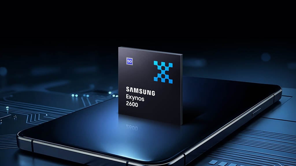
Samsung is mass-producing Exynos 2600 using its 2nm process, and the yields have just hit a turning point. The chip went official last month, and commercialization is set to happen with the Galaxy S26 series next month.
According to ZDNet, Samsung 2nm Exynos 2600 yields hit 50 percent. It’s a significant development that signals the company’s Foundry comeback is real. Samsung is already focusing on the 2nd-gen 2nm process.
With 50 percent yields achieved, the South Korean tech giant is still working to enhance the output. It’s expected to improve sequentially, even though the rate of improvement won’t be that significant compared to TSMC.
TSMC’s 3nm process handed the firm an edge for its 2nm process. The company already has enough orders from major clients like Apple and Qualcomm. Meanwhile, Samsung’s SF2P (2nm process) is gaining traction.
Samsung signed major deals with big tech companies. It’s expected to produce those semiconductors using its enhanced 2nm node. While TSMC is still ahead, Samsung’s next 2nm move is going to be a turning point.
After mastering 3nm, TSMC will now focus on full-scale 2nm production. The industry will welcome the first-generation 2nm products from a variety of vendors, specifically, Apple, Qualcomm, and MediaTek.
Beyond that, TSMC’s roadmap also includes the production of N2P (enhanced N2) in the second half of the year. Reports also indicate that the Taiwanese company aims to explore the production of 16A (1.6nm) this year.
You may like:


Samsung plans to build a new DRAM factory on the Giheung campus in Yongin, which could output around 100,000 wafers per month.
According to KEDGlobal, Samsung is scrapping its R&D ambitions and betting on brute production instead. The company’s new DRAM factory, set to rise on the Giheung campus in Yongin, will crank out 100,000 wafers per month when it’s running.
Korean businessman Lee Byung-chull built it in 1987 and told his people to embrace “infinite exploration.” Samsung demolished it late last year; the plan was to replace it with two R&D buildings but that plan is now dead.
HBM demand has grown so quickly that DRAM makers can’t keep pace, and the shortage is bleeding into commodity chips used in phones and laptops.
Counterpoint Research reports that the global DRAM market revenue is projected to surge from $150 billion (223 trillion won) this year to $210 billion (312 trillion won) due to skyrocketing product prices.
Samsung’s internal team is already formed and eyeing a Q3 groundbreak. The company is even considering tearing down existing Giheung buildings to make room for auxiliary production infrastructure.
The company’s new DRAM factory joins a broader capacity push at Pyeongtaek, where Line 4 is getting a 100,000-wafer-per-month HBM4-capable production line.

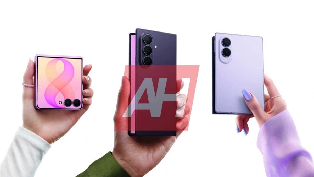
Samsung Flex Titanium is the company’s new foldable-display architecture, pairing a titanium-alloy film with a titanium support plate to cut crease visibility while adding durability. Unveiled today, the technology is officially confirmed to debut in the Galaxy Z Flip 8, Galaxy Z Fold 8, and Galaxy Z Fold 8 Ultra at July 22 Unpacked.
Flex Titanium replaces the polymer film traditionally used inside foldable screens with two titanium-based parts working together:
1. Titanium-alloy Film:
- Sits beneath the OLED panel and measures roughly a third the thickness of a human hair, yet delivers 20 times the mechanical stiffness of the polymer film it replaces.
2. Titanium plate:
- Supports the display module from below. Micro-patterned holes let it flex at the fold while bonding tightly to the module, closing the air gaps that used to sit between the plate and its adhesive.
By swapping in a stiffer, more tightly bonded titanium structure, Samsung says the panel holds a flatter shape across the hinge, so the fold line is far less noticeable in daily use without giving up the flexibility needed for repeated folding.
Samsung hasn’t confirmed a device name or date in this announcement, only that Flex Titanium arrives with its next-generation Galaxy foldables, with specifics saved for Unpacked.
At Unpacked, Samsung will be launching the Galaxy Z Flip 8, Galaxy Z Fold 8, and Galaxy Z Fold 8 Ultra foldable phones. Apple will also drop its first foldable iPhone later this year, which might utilize a similar technology.
That’s the part a quick AI summary won’t tell you. A few things worth weighing before you pre-order:
- Weight and feel: Titanium is stiffer than the polymer it replaces. That helps flatness but can shift in-hand balance; check hands-on impressions, not just spec sheets.
- Manufacturing cost: Precision-rolled titanium is expensive at consumer scale, which may be one reason foldables have stayed premium-priced rather than trending mainstream.
- Repair costs: A titanium-reinforced stack is likely harder, and pricier, to service outside Samsung’s own network.

Samsung Electronics says it is not exploring a U.S. listing through American Depositary Receipts (ADRs), directly rejecting a Bloomberg report that claimed the company had held preliminary talks with banks.
Is Samsung planning a U.S. listing?
No. Samsung has officially denied that it is reviewing a potential US listing.
The clarification, via Reuters, came after a Bloomberg report claimed Samsung was in the early stages of exploring an American Depositary Receipt (ADR) offering.
In a statement to Reuters, a company spokesperson said: “Samsung Electronics is not reviewing the possibility of issuing American Depositary Receipts.” That response leaves little room for interpretation and contradicts Bloomberg’s report.
Unless Samsung changes its position in the future, the answer is straightforward: Samsung is not in discussions on a potential US listing.

Samsung Electronics has reportedly secured an Anthropic AI chip production deal, adding one of the world’s leading AI companies to its growing 2nm foundry customer list.
According to SemiconductorsX, Anthropic is expected to use Samsung Foundry’s 2nm manufacturing process and advanced packaging technologies for its custom AI chips, marking another significant design win as Samsung works to expand its foundry business and narrow the gap with TSMC.
Samsung has reached an agreement to make Anthropic’s proprietary AI chips. While neither company announced the partnership, the reported deal aligns with Anthropic’s broader strategy of developing its own AI silicon.
Anthropic already named Samsung Electronics, SK Hynix, and Micron as strategic partners during its Series H funding round earlier this year.
The chips are expected to be manufactured using Samsung’s 2nm Gate-All-Around (GAA) process alongside the company’s advanced packaging technologies.
The reported Anthropic contract arrives shortly after Samsung’s 2nm momentum gained another boost through Tesla’s AI5 program.
A Samsung Foundry executive recently confirmed that Tesla’s next-generation AI5 chip has entered the tape-out stage, an important milestone before prototype production and yield optimization.
The company was the first foundry to mass-produce 3nm chips using GAA technology, but it has struggled to translate technical milestones into the volume of orders enjoyed by rival TSMC.

Samsung IFA 2026 plans no longer include a large-scale exhibition inside Messe Berlin. Instead, Samsung will host an off-site showcase at Berlin’s Humboldt Carré beginning September 2, two days before IFA officially opens. The venue will be used for product announcements and meetings with media, European retail partners, and B2B customers.
The move follows a similar strategy Samsung adopted at CES 2026, where it skipped the main exhibition hall at the Las Vegas Convention Center in favor of a dedicated space at the Wynn Hotel.
Rather than attracting the largest crowds possible, Samsung appears to be prioritizing a more controlled environment for demonstrating its AI products, connected ecosystem, and business strategy.
Despite leaving the main exhibition floor, Samsung isn’t disappearing from IFA altogether. The company will serve as the main sponsor of the IFA Creator Hub, where it plans to host creator-focused experiences and brand activities inside Messe Berlin.
The decision marks the biggest change to Samsung’s IFA presence in decades.
Aside from the pandemic-affected 2020 event, this will be the first time since Samsung debuted at IFA in 1991 that it won’t operate a major public exhibition at Messe Berlin.
With competitors including LG, TCL, and Hisense maintaining traditional booths, Samsung’s new approach could signal a broader shift in how it participates in global trade shows going forward.
Source – Samsung
-
 Updates22 minutes ago
Samsung rolling out July 2026 update to Galaxy S24, S25, Edge, FE, Fold 7 and more phones
-

 Updates2 days ago
Samsung’s 1.5GB firmware update rolling out to the Galaxy XR headset
-
 Updates2 days ago
Samsung Galaxy S26 grabs July 2026 security update globally
-

 Samsung23 hours ago
Massive promo images leak reveals Galaxy Z Fold 8, Fold 8 Ultra, Flip 8, Watch 9 and Watch Ultra 2 in hero colors