News
Samsung chairman visits Cheonan and Onyang semiconductor package plants
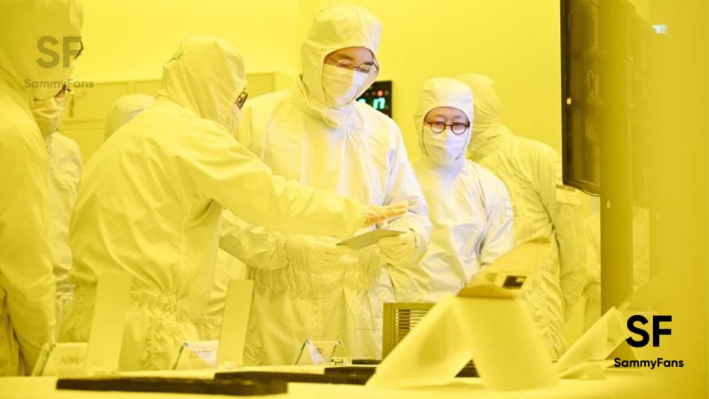
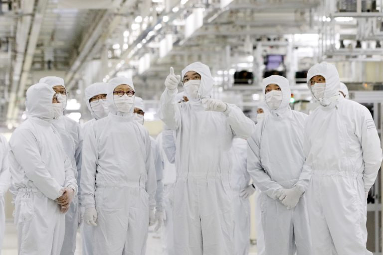
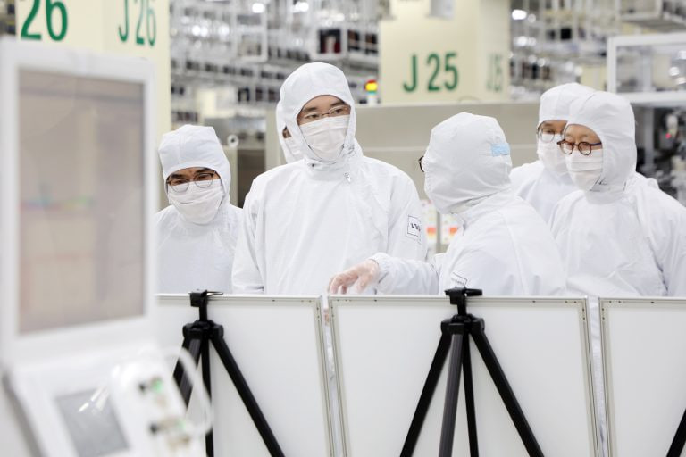
On February 17, the chairman of Samsung electronics – Lee Jae-yong visited the company’s semiconductor package plants in Cheonan and Onyang campuses. He oversaw mid-to-long-term business strategies, along with next-generation package competitiveness and R&D capabilities.
Alongside the chairman, many other Samsung heads, such as the head of the DS Division – Kyung Kye-hyun, the head of the Memory Business Division – Jung-bae Lee, the head of the Foundry Business Division – Siyoung Choi, and the head of the System LSI Business Division – Yong-in Park have also attended the management meeting in Cheonan Campus.
Follow our socials → Google News, Telegram, Twitter, Facebook
The Samsung chairman personally inspected the semiconductor production line where advanced package technologies such as HBM (High Bandwidth Memory) and WLP (Wafer Level Package) are implemented.
He requested, “Although it is a difficult situation, there should be no wavering in talent cultivation and future technology investment.”
For your information, Semiconductor packaging is a process of manufacturing semiconductors in a form suitable for electronic devices. It is a technology with high-performance and low-power characteristics in various fields such as AI, 5G, and electric vehicles.
The importance of advanced package technology is increasing day by day as an alternative to overcome the miniaturization limit of semiconductor circuits to less than 10 nanometers.
Moreover, Samsung employees who attended the meeting spoke about the pride they felt as developers, the goals of new technology development, and complaints. At the same time, the Chairman expressed his gratitude for the dedication and efforts of the officers and employees.
On the other hand, Lee also visited local business sites, inspected the business situation, and continued to communicate with local small and medium-sized businesses.


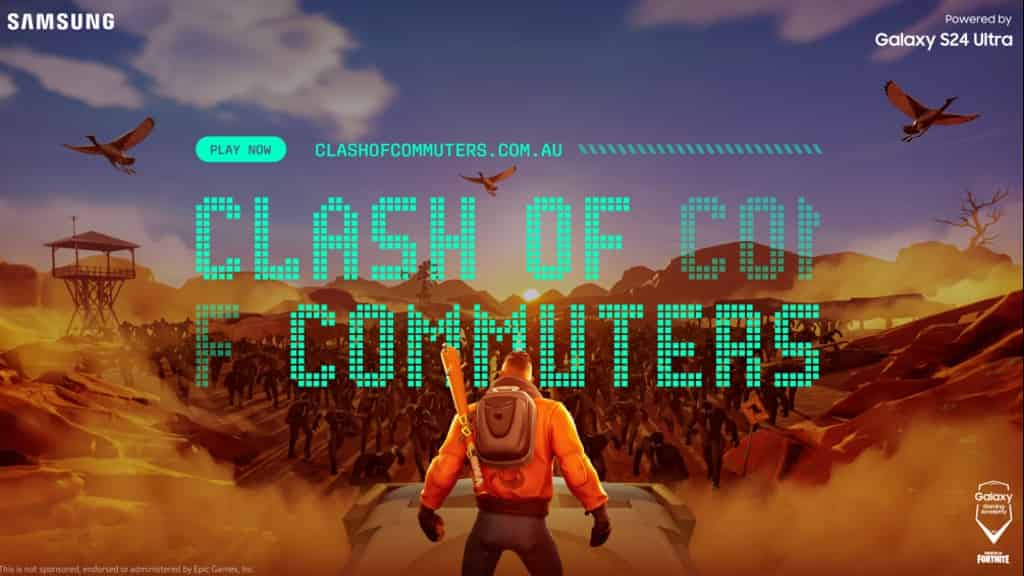
Samsung announced Clash of Commuters on Fortnite in Australia. This new experience features Australian icons from the humble Bin Chicken to a Sydney train to let gamers play a uniquely Australian and public transport-inspired map in Fortnite Creative.
Players can also win Samsung swag IRL by participating in the Clash of Commuters until May 30. To be a winner, gamers have to defend an Aussie public bus across 5 checkpoints as it meanders through a dystopian commute, complete with bin chickens, servos, and caffeine-starved commuters.
Samsung’s new Clash of Commuters map enables players to experience an all-new Fortnite Creative island. It also allows them to defend the very thing that they commonly game on. Pay attention, 44% of Aussie gamers admit they game while commuting to pass the time.
Activation opening times:
- Parramatta Square, NSW: 4 to 8 May, 11am to 7pm daily
- Southern Cross Station, VIC: 11 May to 15 May, 11am to 7pm daily
Image: Samsung
The player who completes all five rounds of the Clash of Commuters campaign in the shortest amount of time (The Shortest Haul) will be eligible to win a Samsung gaming pack worth over $8,000, which includes a 55” OLED TV, Odyssey OLED G9 Monitor, Galaxy S24 Ultra and Galaxy Buds2 Pro.
There will also be additional prize packs for the fastest player to complete the campaign on a mobile device (The Ultimate On-The-Go Gamer), the most side quest phones acquired (Seat Scavenger), as well as four winners drawn at random from all completed time submissions (Regular Riders).
Stay up-to-date on Samsung Galaxy, One UI & Tech Stuffs by following Sammy Fans on X/Twitter. You can also discover the latest news, polls, reviews, and new features for Samsung & Google Apps, Galaxy Phones, and the One UI/Android operating system.
Do you like this post? Kindly, let us know on X/Twitter: we love hearing your feedback! If you prefer using other social platforms besides X, follow/join us on Google News, Facebook, and Telegram.
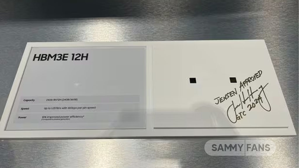
Samsung formed a team for a billions-of-dollars HBM supply deal with Nvidia. The company is putting efforts into winning the contract from the global artificial intelligence semiconductor giant to beat the HBM market leader SK Hynix.
According to KEDGlobal, Samsung made a task force to finalize its HBM deal with Nvidia. The team comprises about 100 excellent engineers, who have been working to improve manufacturing yields and quality with the first aim to pass Nvidia’s tests.
“Samsung aims to log a high market share by quickly increasing supply to Nvidia,” said one of the sources. “It is expected to speed up the supply from the third quarter.”
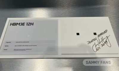
Previously, Nvidia CEO Jensen Huang asked Samsung Elec to increase the yields and quality of 8-layer and 12-layer HBM3E chips for supply. It’s worth noting that HBM3E is the world’s best-performing DRAM chip for AI applications.
36Gb 12-layer HBM
The South Korean tech giant has been focussing on the 36Gb 12-layer HBM3E model. Samsung finished the development of HBM3E in February 2024 and aiming to pass the quality test conducted by Nvidia this month.
To meet Nvidia’s demand, the company has secured production lines already to increase output. The 12-layer HBM3E improves AI learning speed by 34% on average compared to the 8-layer product.
Stay up-to-date on Samsung Galaxy, One UI & Tech Stuffs by following Sammy Fans on X/Twitter. You can also discover the latest news, polls, reviews, and new features for Samsung & Google Apps, Galaxy Phones, and the One UI/Android operating system.
Do you like this post? Kindly, let us know on X/Twitter: we love hearing your feedback! If you prefer using other social platforms besides X, follow/join us on Google News, Facebook, and Telegram.
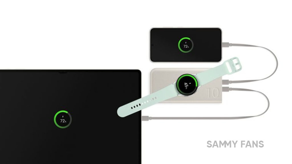
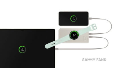
Samsung released new battery pack products in India, featuring up to 20,000mAh capacity and 45W speed. In particular, the company announced two different models: 10,000mAh capacity with 25W charging and 20,000mAh with 45W charging.
Selling on Samsung.com and Amazon, Samsung’s new battery packs are available in a Beige colorway. As far as the pricing is concerned, the new 10,000mAh battery pack costs INR 3,499 while the 20,000mAh battery pack is priced INR 4,299.
Samsung’s 20,000mAh pack comes with many advantages including triple port capability, letting users charge up to three devices simultaneously. It gives users peace of mind as charging a phone alongside a smartwatch and earbuds or tablet is simpler and easier.
The 10,000mAh battery pack features 25W Superfast Charging. It has dual port functionality, allowing users to charge two different devices at once. The company notes that the power banks are made with UL-certified recycled materials which help reduce carbon emissions.
[Via]
Stay up-to-date on Samsung Galaxy, One UI & Tech Stuffs by following Sammy Fans on X/Twitter. You can also discover the latest news, polls, reviews, and new features for Samsung & Google Apps, Galaxy Phones, and the One UI/Android operating system.
Do you like this post? Kindly, let us know on X/Twitter: we love hearing your feedback! If you prefer using other social platforms besides X, follow/join us on Google News, Facebook, and Telegram.