
Semiconductor
NVIDIA changes the HBM formula, and Samsung is adapting


Samsung is reportedly developing an 8-layer version of its HBM4E memory specifically for the NVIDIA NVHBM platform, marking a notable shift in how high-bandwidth memory could be designed for next-generation AI systems.
According to SEDaily, NVIDIA has asked Samsung to tailor its seventh-generation HBM4E around an 8-layer configuration for NVHBM, rather than the taller 12-layer and 16-layer stacks the company has been preparing.
The custom memory is also expected to target speeds of 17 to 18Gbps per pin, significantly above Samsung’s initial HBM4E sample specification of 16Gbps.
NVIDIA officially introduced NVHBM this week as part of its NVLink Fusion strategy. The company appears to be taking a different route for NVHBM, prioritizing speed, physical efficiency, and supply scalability.
NVHBM architecture moves the memory controller into the HBM base die, freeing space on the XPU while enabling up to 30% higher memory bandwidth and 15% lower HBM power consumption compared with standard HBM4E.
Samsung could benefit from this design direction because its semiconductor business combines DRAM, logic, advanced packaging and foundry capabilities.
The 8-layer NVHBM is reportedly being considered for NVIDIA’s future AI platforms, including the Vera Rubin Ultra generation.


US media outlets reported that the Donald Trump administration is considering imposing heavy tariffs on semiconductor products, as well as finished products containing them.
According to a report by Politico on August 27, the plan under consideration by the U.S. government significantly expands the scope of products subject to semiconductor tariffs.
This expansion could cover not only semiconductors themselves but also various finished products that contain them, such as mobile devices, laptops, gaming consoles, and data center servers.
Politico reported that ideas being discussed include setting country-specific tariff rates and quotas, as well as applying country-specific guidelines targeting major semiconductor manufacturers.
However, it is understood that this initiative could be substantially modified over the coming months, and Commerce Department officials have yet to finalize details such as exact tariff rates.
Sources said US Commerce Secretary Howard Lutnick favors a structure that promotes domestic production by tying tariff exemption benefits for foreign companies to semiconductor manufacturing investments within the United States.
The US government has been imposing semiconductor tariffs on a very small set of specific products since January, while signalling the possibility of extending tariffs to semiconductors overall in the future.


Intel showed its latest chip technology at the Hot Chips 2026 event. The company presented three new products: Diamond Rapids, Crescent Island, and Wildcat Lake. These products show that Intel is improving its chip-making technology to compete with companies such as TSMC, Samsung, Nvidia, and AMD.
The main highlight was Diamond Rapids. It is Intel’s next-generation Xeon server processor and is expected to launch in 2027. It will be the first server processor made using Intel’s improved 18A-P manufacturing process.
Diamond Rapids is designed for businesses that use AI. Intel says the chip will provide better performance, use less power, and handle large workloads more efficiently. It will also offer better memory and connection features.
Intel’s 18A technology is an important part of its plan to improve chip production. It uses a new transistor design, RibbonFET and a new power system called PowerVia. Intel is producing these chips at its new Fab 52 factory in Arizona, USA.
The company is already using 18A technology in several products. These include Panther Lake processors for laptops and Wildcat Lake chips for regular computers and small businesses. Intel has also used the technology in its Arc G3 and Arc G3 Extreme handheld processors.
In the server market, Intel introduced Clearwater Forest, also known as Xeon 6+, earlier this year. It was the company’s first server processor made using 18A technology. With Diamond Rapids, Intel is bringing its 18A technology to more powerful server chips.
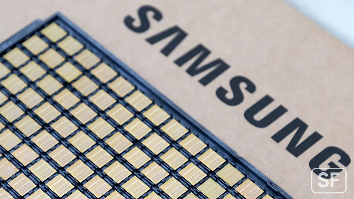
Samsung is exploring a major shift in how HBM works in AI systems. Instead of functioning mainly as a high-speed data store for GPUs and other accelerators, future HBM could take over memory-control tasks and even perform selected AI operations.
Samsung wants HBM to do more than move data
Samsung’s DRAM engineers are looking at the logic base die inside HBM as an opportunity to add more functionality. Modern HBM uses an advanced logic layer beneath its stacked DRAM dies, and Samsung has increasingly moved toward sophisticated base-die technology.
Under the proposed architecture (via Maeil Business), the memory controller could move from the GPU into the HBM base die. Samsung believes this could free valuable space inside the processor for additional compute resources while improving overall system performance.
The more ambitious concept is called aHBM, where the memory itself handles selected AI operations.
Rather than sending data back and forth to the GPU for every memory-intensive task, some processing could happen closer to where the data resides. This could reduce data movement and, importantly, lower power consumption.
Thermal constraints remain a challenge, since putting more processing into an HBM base die also generates additional heat. Samsung therefore sees selective workloads, particularly those involving heavy memory access, as the more practical starting point.
This approach fits into Samsung’s broader push toward 3D AI memory. At FMS 2026, the company unveiled zHBM. Samsung says the architecture could eventually deliver roughly 8x the performance of HBM5 while improving energy efficiency.


AI chips are becoming more powerful, but moving data between chips is becoming a major problem. To solve this, companies are developing Co-Packaged Optics (CPO), which uses light to move data faster. SK Hynix is now entering the CPO market.
SK Hynix wants to combine CPO with HBM and memory-pooling technology to improve the performance of AI systems. However, it will need important technologies from TSMC to make this plan successful. TSMC has three key technologies: COUPE, SoIC, and CoWoS.
COUPE connects electronic chips with optical chips. SoIC allows chips to be stacked on top of each other, while CoWoS helps combine processors, HBM, and optical parts into one package.
But CPO needs more than chip technology. It also requires optical fibers, tiny lenses, accurate alignment, packaging, and testing. This is creating new opportunities for Taiwanese companies.
Sung-Chuan makes Fiber Optic Array Units that connect optical fibers with silicon photonics chips. It is developing products with speeds of 1.6T, 3.2T, and eventually 6.4T. Largan Precision is developing small optical parts and fiber arrays for CPO. It could begin mass production as early as 2027.
Xunxin-KY is focusing on CPO packaging. Its 51.2T product has already reached small-scale production, while its 102.4T product is being tested. SK Hynix wants to enter the CPO market, but TSMC and other Taiwanese companies provide many of the important technologies needed to make it work.

Samsung could have another route to challenge China’s growing memory chip industry, including CXMT products, in the US, following fresh testimony in South Korea over alleged theft of its DRAM manufacturing technology.
A former Samsung engineer who joined ChangXin Memory Technologies (CXMT) has reportedly testified that the Chinese memory maker sought Samsung’s proprietary process know-how during its early development.
The testimony is significant because prosecutors have alleged that Samsung’s 18-nanometer DRAM technology was obtained and subsequently adapted for CXMT’s manufacturing operations.
The disputed technology covers Samsung’s Process Recipe Plan, a highly detailed set of manufacturing instructions spanning hundreds of production steps.
If the Korean court ultimately accepts the testimony and other evidence, Samsung could potentially use the findings in future legal action against CXMT.
One possible avenue is the US International Trade Commission (ITC), which can restrict imports of products found to violate Section 337, as per Pulse Korea.
Samsung’s earlier case against Chinese display maker BOE produced a recommended 14-year-and-eight-month exclusion order before the broader dispute was ultimately terminated following a settlement.
For CXMT, however, a future Samsung complaint would still need to establish the required legal connection between the alleged trade-secret misuse and imported products. A US ban is therefore a possibility, not an outcome at this stage.
If Samsung succeeds, it could significantly complicate CXMT’s ambitions to expand its presence in the global DRAM market, particularly in the United States.
-
 One UI10 hours ago
One UI 9.0 (Android 17) testing on these 68 Samsung devices
-
 One UI2 days ago
Samsung’s August 2026 update released for Galaxy S26, S25, S25 FE, S24, Flip 6, Fold 7, and Flip 7
-
 Samsung2 days ago
Samsung confirms Android and iOS requirements for One UI 9 data transfer feature
-
 News2 days ago
iPhone 17 Pro and Galaxy S26 Ultra were the Q2 bestsellers worldwide