
Semiconductor
Samsung using HBM4 supply as leverage to win AMD chip manufacturing business


Samsung appears to have found a way to turn its HBM4 memory shortage into a bargaining chip, and AMD is the one sitting across the table.
When Lisa Su landed in Seoul on October 7, the stated agenda was high-bandwidth memory. AMD’s Helios rack needs 31TB of HBM4 per system and cannot ship without it.
Per TrendForce and Chosun Biz, the same meetings also touched on a bigger question: whether Samsung Foundry can finally pull AMD’s CPU and GPU dies onto its SF2P 2nm process. No contract has been announced, and the terms remain undisclosed.
The leverage is easy to see. SK Hynix has reportedly committed most of its 2026 HBM4 output to NVIDIA, which leaves Samsung as AMD’s primary supplier for the Instinct MI455X.
Samsung has wanted AMD’s logic business since its 14nm work for the company in 2016, before everything advanced moved to TSMC.
AMD isn’t racing to say yes. An AMD executive reportedly called TSMC the undisputed leader at 2nm, and Korean media cited an industry official describing a Samsung move as “too risky.”
Yield is the sticking point, since Samsung’s SF2 is reportedly well short of the roughly 70 percent that high-volume customers expect.
AMD can’t hand Samsung its flagship accelerators any time soon. A consumer Ryzen part is the safer first step, and Daishin Securities has hinted at something along those lines.
Chair Su did say AMD “continues to explore partnership opportunities,” which is diplomatic for “not yet.” Even so, the dynamic is hard to ignore; AMD invented HBM, yet it can’t make a single stack, and Samsung knows it.








Samsung Elec’s memory business is doing excellently, but Q3 2026 numbers for the foundry side told a very different story.
In Q3, Samsung’s chip business had a record quarter, just not in the part that makes chips for other companies. The DS Division carried the third quarter on AI memory demand, helping Samsung climb past $80 billion in operating profit.
According to a report from ZDNet, the non-memory unit, which covers foundry and System LSI, likely lost around 2 trillion won.
Analysts point to one-time costs from the new US fab and performance bonuses, even as utilization rates inch upward. Revenue is the bigger worry; IBK Securities estimates about 6.7 trillion won, barely above the previous quarter and a year earlier.
TSMC, meanwhile, reported revenue of 1.49 trillion New Taiwan dollars, up 51% year over year and 17% on the quarter. TrendForce had TSMC at 72.5% of foundry revenue in Q2, while Samsung slipped to 5.9% from 6.5%. Q3 almost certainly widened that spread.
Samsung’s 4nm lines are busy, reportedly serving logic dies for AI chips and HBM. The industry sees 2nm customer wins as the real test. Flat revenue during an AI boom suggests Samsung is not capturing the demand TSMC is.
One major 2nm customer could change the mood quickly, but without it, the US fab may start to look like an expensive bet placed ahead of the orders.

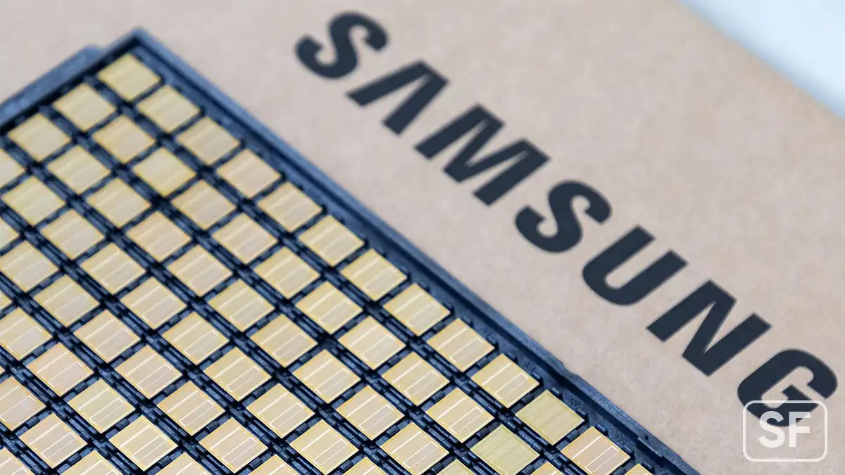
Samsung and SK Hynix could continue benefiting from strong demand for HBM4, as the next-generation NVIDIA Rubin AI platform is expected to retain 12-layer memory stacks despite concerns about rising production costs.
According to Counterpoint Research, most HBM4 chips used in NVIDIA Rubin AI accelerators are likely to maintain the 12-layer configuration. This challenges earlier speculation that NVIDIA might reduce stacking to eight layers to manage costs.
NVIDIA may avoid an HBM4 layer reduction
HBM4 requires significantly more manufacturing capacity than conventional DRAM, meaning sustained demand can keep production resources tied up and limit the supply available for other memory products.
Counterpoint also pushed back against expectations that four-layer HBM products would gain traction in the custom AI chip market.
The market research firm said it had not identified such products in the ASIC segment, suggesting that performance and memory capacity remain priorities for AI infrastructure providers.
For Samsung, that could provide another source of momentum as it ramps up HBM4 production. If Nvidia maintains its preference for higher-capacity stacks, memory suppliers may face less pressure to scale back production requirements.
Strong HBM demand can constrain manufacturing capacity for general-purpose DRAM, potentially supporting prices while AI infrastructure investment continues.
Samsung recently reported preliminary third-quarter 2026 revenue of 195 trillion won and operating profit of 107.4 trillion won (roughly $80 billion).
If the 12-layer configuration holds, Samsung could retain a valuable opportunity in the HBM4 market. For now, however, the outlook remains an industry forecast.


Samsung is making a potentially important move in the next generation of AI memory, with its 12-layer HBM4E reportedly clearing quality verification with NVIDIA and major hyperscale customers.
According to Korean outlet Hankyung, Samsung Electronics’ Memory Business Division completed the qualification process late last month.
Passing these tests means the memory has met the technical and reliability requirements set by key customers, although there is still no confirmed information on supply volumes, contract sizes, or mass-production schedules.
Samsung began mass-producing HBM4 in February and shipped 12-layer HBM4E samples to global customers in May.
The company did not identify those customers, but NVIDIA and major hyperscalers were widely considered likely recipients.
Samsung’s 12-layer HBM4E stacks 48GB of memory and reaches speeds of up to 16Gbps per pin. Samsung claims a 16% improvement in energy efficiency through its low-power design and optimized packaging.
The memory uses Samsung’s 1c DRAM process alongside a 4nm logic die from Samsung Foundry, maintaining the same basic process combination used for its HBM4 production.
For Samsung, securing customer qualification this early could prove significant. Still, qualification is not the same as a confirmed supply deal.
Samsung has not publicly confirmed the reported NVIDIA verification, and the company continues to keep customer-specific qualification details private.

Samsung Electronics is reportedly nearing the final stage of negotiations with Nvidia and Broadcom over HBM4 supply for 2027, with the company seeking prices that could be more than double current HBM levels.
The reported push comes as Samsung shifts its high-bandwidth memory business from HBM3E to HBM4. Chosun Biz reports that Samsung has already secured a substantial portion of next year’s orders from major customers, including Nvidia and Broadcom, leaving the remaining negotiations largely focused on pricing.
Market forecasts support the possibility of a sharp increase. KB Securities expects Samsung’s HBM selling prices to rise by more than 100% next year, while TrendForce has projected an average HBM price increase of 121%.
The broader memory market is helping strengthen Samsung’s position. General-purpose DRAM prices remain under pressure from tight supply, while larger HBM dies are consuming more wafer capacity with each generation.
Micron’s reported success in securing much of its 2027 HBM supply at higher prices could give Samsung and SK Hynix additional room to push negotiations upward.
Hana Securities estimates HBM could account for around 15% of Samsung’s DRAM revenue next year, with some market scenarios putting that figure considerably higher if HBM4 prices double.

Samsung is expanding its semiconductor footprint in Vietnam with a new large-scale memory test facility in Thai Nguyen, adding another overseas node to its increasingly diversified chip supply chain.
Established in March, Samsung Vietnam Semiconductor (SVS) is building the facility inside Yen Binh Industrial Park, close to Samsung’s existing smartphone manufacturing operations. The site covers roughly 265,895 square meters, with the project planned in two phases.
The first production line is scheduled to receive equipment from July 2027 and start operations in the fourth quarter of that year. A second line is expected to begin equipment installation in May 2028 before entering operation in October.
Unlike a wafer fabrication plant, the facility will handle backend testing of packaged DRAM and NAND. Samsung uses this stage to verify memory performance, reliability, and error rates before products are shipped to customers.
Samsung plans to fund much of the expansion through profits generated locally rather than relying heavily on external borrowing.
The Korean tech giant is also training 103 Vietnamese engineers at its Cheonan and Onyang semiconductor facilities, suggesting the company is preparing the workforce well ahead of mass production.
This signals a broader shift in Samsung’s Vietnam strategy. The country is moving beyond being primarily a smartphone assembly hub and becoming a more meaningful part of Samsung’s semiconductor supply chain.
-
 One UI2 days ago
One UI 9.0 official update now rolling out to these Samsung phones
-

 One UI3 days ago
Galaxy Watch 7 and Watch 6 receive One UI 9 Beta 3 update fixes
-
 News3 days ago
Samsung updates One UI software rollout roadmap – October 2026
-

 One UI3 days ago
Samsung Galaxy A54 receives One UI 9 Beta 2 with October 2026 patch