Technology
Samsung ISOCELL HP2 200MP Camera Technology Analysis
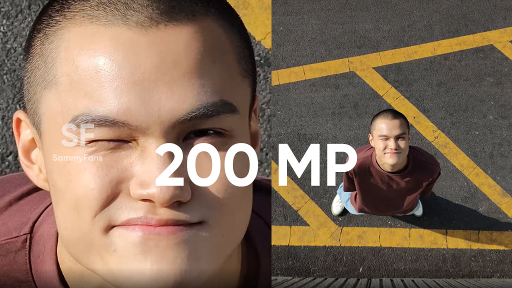
Samsung recently unveiled a 200MP ISOCELL HP2 camera sensor with improved pixel technology to capture beyond pro-level photos in ultra-high resolution. Samsung Galaxy S23 Ultra smartphone is going to have this powerful camera sensor.
Follow Sammy Fans on Google News
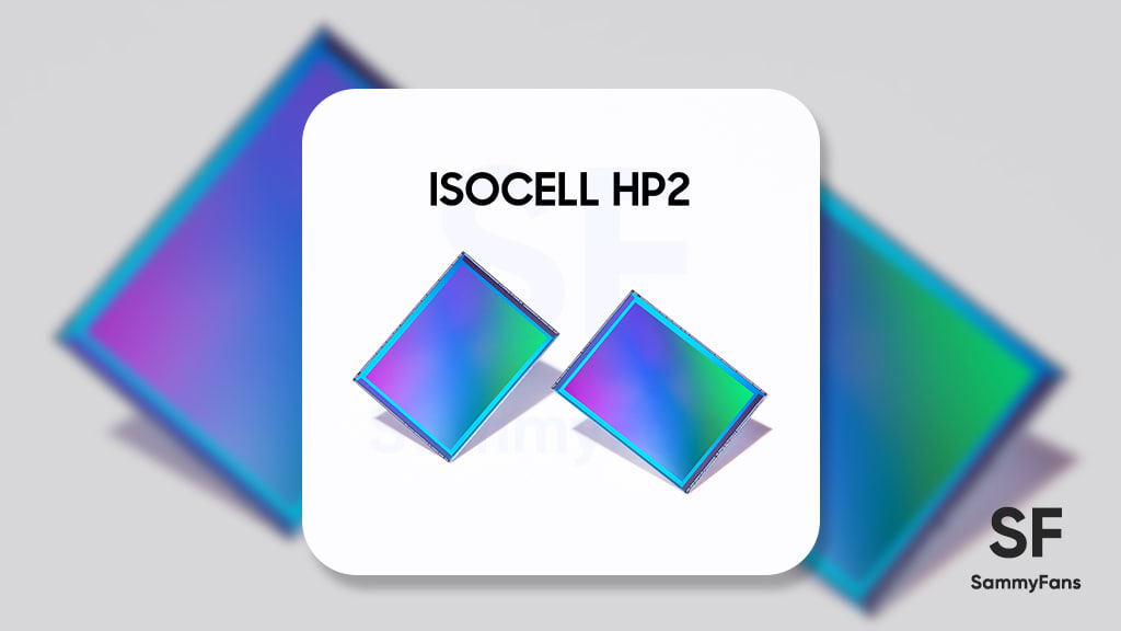
Through Samsung’s 200MP HP2 camera sensor, the company is pointing to a different tech tree this time around. It is most likely Galaxy S23 Ultra main camera CMOS with a size of 1/1.3 inch, 200MP 16 in 1, and a single pixel of 0.6μm. However, we’re not surprised by the size, let’s check other perspectives.
Join Sammy Fans on Telegram
D-VTG Technology
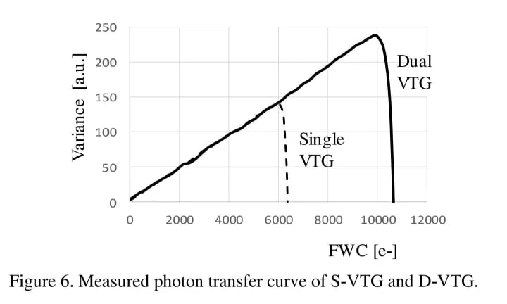
HP2 camera sensor adopts D-VTG (Dual vertical transfer gate) technology that greatly increases the full well capacity (FWC) of a single pixel. The well capacity is 33% higher than the previous generation ISOCELL. Most importantly, the smartphone’s CMOS with limited planar size, especially the HDR highlight suppression and the signal-to-noise ratio under sunlight.
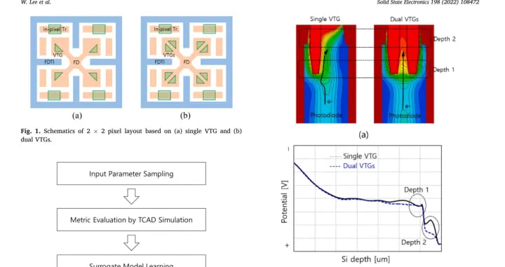
The HP2’s D-VTG technology appeared in a paper published by Samsung in the Journal of Solid State Electronics. A transmission gate TG corresponding to the photodiode PD is changed into two, and the TG is placed vertically with respect to the PD, which is called a Dual VerticalTransfer Gate.
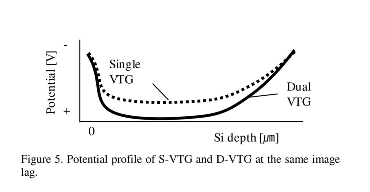
The benefit of D-VTG technology is that it not only has better conduction efficiency because TG controls the flow of electrons from PD to FD but it may well also increase the potential difference of charge, thereby increasing the maximum number of electrons that PD can carry.
Samsung designed a single pixel with 6,000 electrons, which has been increased to 9,000 electrons through the new technology, i.e., 1.5 times the maximum consumption, compared to the 33% improvement currently advertised by HP2.
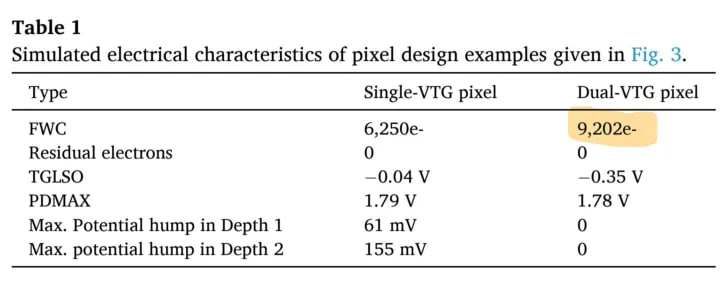
Samsung HP2 200MP camera sensor is a full well of 10,000 electrons in a single pixel. It is important to note that the pixel size of A7R4/R5 is very large, and there are only 36,000 electrons in a full well.
Dual Slop Gain
Samsung introduced Dual Slope gain technology in the ISOCELL HP2 for the first time in Samsung’s image sensor lineup to take HDR for high-resolution images to the next level. In all pixels, it applies two different conversion values when light is converted into a digital signal.
The “two different conversion values” mentioned by Samsung are actually the readout capacity of the two FD areas, one larger and one smaller, and the smaller capacity corresponds to the higher conversion gain, the higher the conversion gain.
Conversion gain can be seen as slope, that is voltage converted into a unit of electron energy and the unit is mV/e-, which is the origin of slope in propagation.
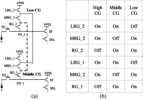
It is actually mentioned that the FD field capacitor is switched to switch the conversion gain, but Samsung’s paper shows three capacitors playing a three-gain TCG. Sadly, in the current state, HP2 is not installed.
200 MP and Focus
The HP2 really is the right direction for mobile photography. It’s not that the HP2 has more pixels, but Samsung chose to grow the sensor vertically so it has a chance to compete with an inch, especially since the bottom half of the phone is usually equipped with a larger aperture.
HP2’s 200 million pixels is the equivalent of 4 in 1 5000w pixels, divided into four grids for Quad PD focusing, i.e. tilt and horizontal/vertical phase can be detected.
HP2 is the most balanced main camera CMOS at present. It should be considered a 50mp four-in-one, but each tiny pixel has its own focus function, as its DSG function can’t be turned on at 200mp. Meanwhile, reading speeds at 200mp are just 15fps, which is pretty low for a stack-heavy phone.


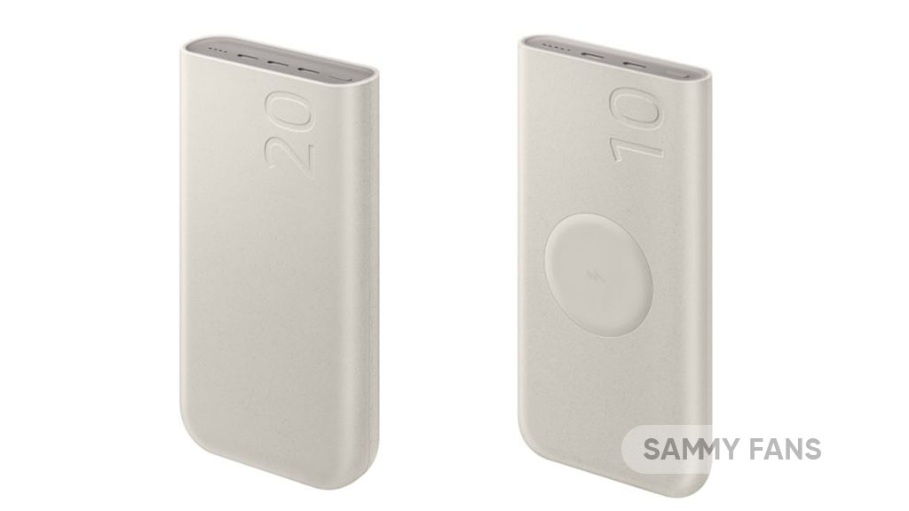
Samsung has unveiled two new battery packs with powerful performance using recycled materials. The launch, scheduled for the 19th, introduces the PD Battery Pack 20,000 mAh and the PD Wireless Charging Battery Pack 10,000 mAh. Both of these battery incorporate 30% UL-certified recycled plastic in their design, marking a stride in reducing carbon emissions.
The ‘PD Battery Pack 20,000 mAh’ offers a high capacity for charging, with a maximum output of 45W and three USB-C ports, allowing for simultaneously charging multiple devices. However, the actual charging speed may vary based on several factors, including the devices connected and charging conditions.

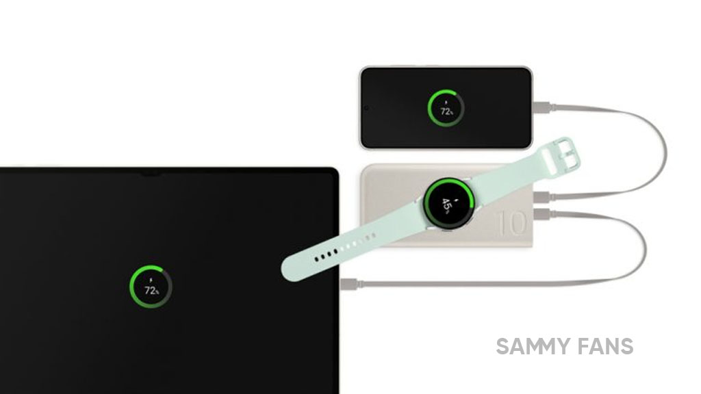
On the other hand, the ‘PD Wireless Charging Battery Pack 10,000 mAh’ provides the convenience of wireless charging, along with a wired charging capability of up to 25W. It comes with two USB-C ports, making it possible to charge up to three devices at once when combining wired and wireless charging.
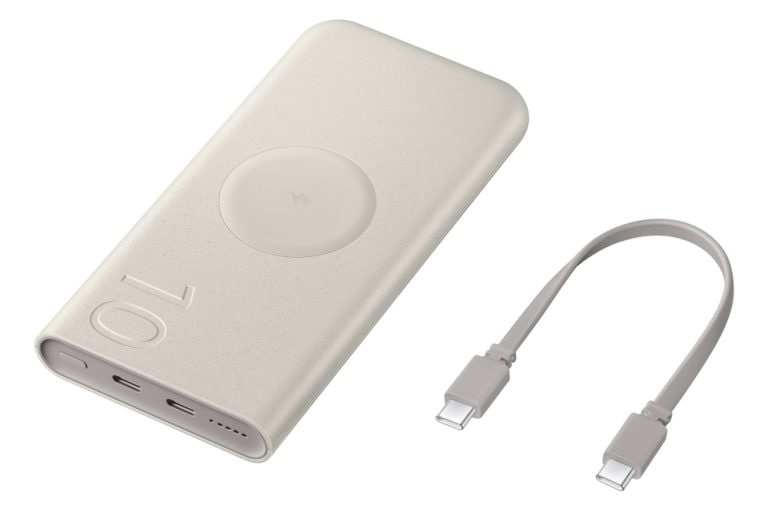
Both battery packs comply with the USB PD 3.0 standard, ensuring quick and efficient charging for Samsung Galaxy products and other compatible devices.
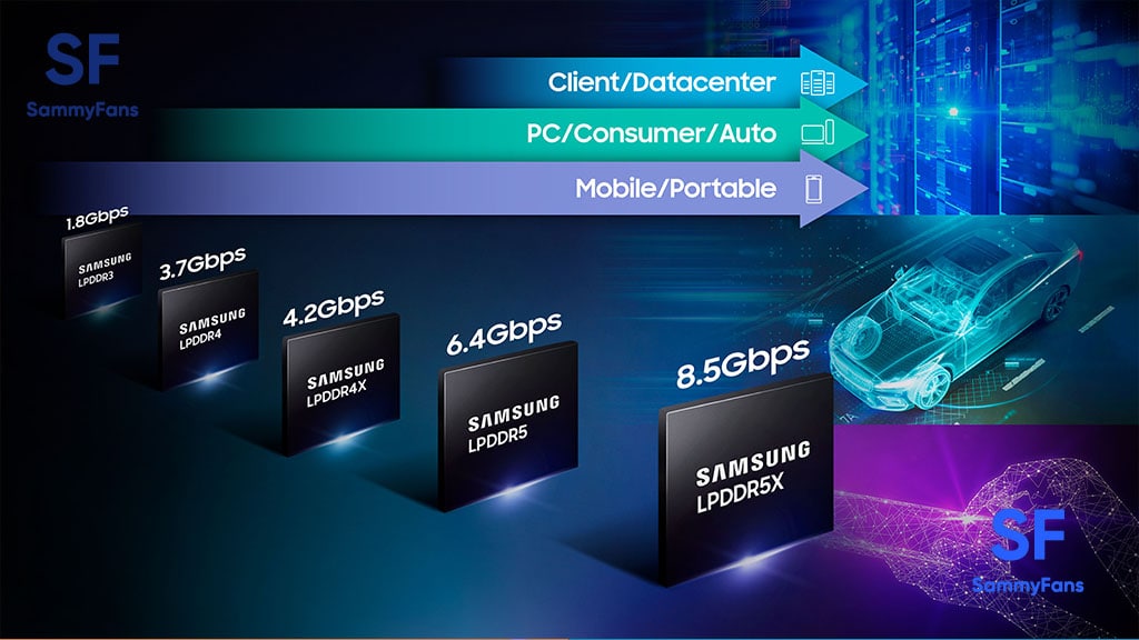
The LPDDR6 market is expected to bloom as early as next year, as the new on-device AI memory is on the way with the latest LPDDR6 standard finalization taking place in Q3 2024. If the standard is confirmed in the third quarter, LPDDR will secure a new standard for the first time in five years.
Going toward the details, the International Semiconductor Standard Organization (JEDEC) recently held discussions on the next-generation mobile RAM standard. The meeting proceeded with the finalization process to finalize the LPDDR6 standard.
An official in the semiconductor industry said,
- “We have held various discussions to confirm the LPDDR6 standard specification,” and it will be released in the third quarter of this year.”
To be mentioned, the JEDEC is a private organization that establishes semiconductor standards, that is, sizes and specifications, and more than 60 people from memory, system semiconductor, and design asset (IP) companies participated in this Lisbon meeting.
Follow our socials → Google News | Telegram | X/Twitter | Facebook | WhatsApp
Furthermore, the LPDDR6 standard will be established with a focus on improving data processing performance as the demand for on-device AI to perform large-scale AI calculations on smartphones, laptops, and tablet PCs is rapidly increasing. In addition, the power consumption standard will also be improved.
However, once the LPDDR6 standard is confirmed, major memory manufacturers such as Samsung Electronics and SK Hynix are expected to begin commercializing their products in earnest.

Microsoft has announced the launch of a new AI chatbot that can help finance workers with common tasks in Excel and Outlook. The Copilot for Finance is currently in public preview and will be available for purchase soon.
The Copilot for Finance is part of Microsoft’s vision to empower every department with a Copilot, a smart assistant that can generate natural-sounding text or other content with minimal human input.
Follow our socials → Google News | Telegram | X/Twitter | Facebook | WhatsApp
As per the information (via CNBC), the Copilot for Finance can perform functions such as variance analysis, data reconciliation, and collections process in Outlook, using data from SAP and Microsoft Dynamics 365. Microsoft plans to add more features to the Copilot for Finance later this year.
Microsoft’s corporate vice president Charles Lamanna said that the Copilot for Finance was developed with input from Microsoft’s finance department. He also said that the Japanese advertising agency Dentsu will be one of the first customers to use the Copilot for Finance.