
Semiconductor
Galaxy S27’s 2nm Exynos 2700 beats Snapdragon rival by 20% in Geekbench and Graphics tests


Samsung’s bet on its in-house mobile chip is paying off. Internal tests suggest that the upcoming Exynos 2700 has surpassed its Snapdragon rival by 20% in Geekbench and Graphics benchmarks ahead of the Galaxy S27 launch.
Galaxy S27, S27+, and S27 Pro are expected to launch with Exynos 2700 in the majority of countries. Samsung is reportedly considering utilizing its in-house SoC in the Ultra model too, but that is not finalized yet.
Exynos vs Snapdragon – Geekbench
Exynos 2700
Information shared by SemiconductorsX suggests that Exynos 2700 scored 13,000 in Geekbench 6.5’s multi-core test. The device used for this test is unknown, but it appears to be a Galaxy S27 Pro, the newly added model.
- Exynos 2700: 13,000 multi-core score (as of October 25)
Snapdragon 8 Elite Gen 6
Qualcomm’s 2nm-based Snapdragon 8 Elite Gen 6 has been surpassed by Samsung’s Exynos 2700, with 44% higher multi-core scores in Geekbench 6.5. The gap changed to 36% when the Geekbench 7.0 platform was adopted for testing.
Snapdragon 8 Elite Extreme Gen 6
Xiaomi 18 Pro Max, which uses Snapdragon 8 Elite Extreme Gen 6, scored nearly 11,000 on the same benchmark. Comparing the scores of the two devices reveals a difference of 2,000 points, or 15% on Geekbench 7.0.
The results came from recent in-house benchmark tests comparing the Exynos 2700 with Qualcomm’s Snapdragon 8 Elite Extreme Gen 6, which powers Xiaomi’s 18 Pro Max, according to industry sources on Sunday.
Samsung plans to launch its flagship Galaxy S27 lineup in late January or early February next year. The company and its Exynos arm still have a significant period for further optimization, which will ramp up performance.
“Development of the Exynos 2700 is on track, with the aim of having it used in flagship models,” Park Yong-in, president and head of the System LSI Business, said at a management briefing in June.
Samsung’s memory division is printing money on scale, thanks to DRAM and HBM sales. However, the non-memory (chip manufacturing business) weighing on Exynos 2700 to turn deficit into profitability as soon as Q1 2027.




MediaTek has reportedly reduced token limits for its AI tools used by engineers, highlighting the challenge of controlling costs as AI usage increases. In response, the company said it would automatically select different AI models based on task complexity to improve efficiency and manage growing demand.
Tokens are the basic units of text processed by AI models. The more AI tools are used, the more tokens they may consume, which can increase costs for businesses.
MediaTek’s approach shows how companies can control AI expenses by using the right model for each task. Simple tasks can be handled by less expensive models, while more complex tasks can use advanced models when needed. This helps companies balance cost and performance.
Businesses should not focus only on the price of AI tools. They should measure the total cost of completing a task and compare it with the benefits received. Although newer AI models may cost less per task, overall spending can still increase as employees use AI for more activities.
Companies should also identify repetitive tasks that AI can handle, improve existing work processes, and measure the results of AI adoption. Monitoring expenses across departments can help businesses understand where their money is being spent.
At the same time, businesses must protect sensitive data and set clear rules for how AI tools operate. Maintaining good-quality company data is also important for achieving better results.
MediaTek’s reported decision highlights an important lesson for businesses: controlling AI costs does not simply mean reducing usage. It means choosing suitable models, using tokens efficiently, and ensuring that AI delivers real value.


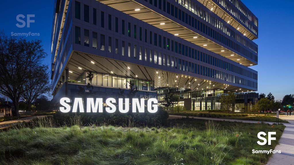
Samsung Electronics is quietly wrapping up the core puzzle pieces for its Taylor 2nm semiconductor manufacturing fab in Texas, targeting up to 20,000 2nm wafers produced by the second half of 2027.
According to ZDNet, Samsung has recently placed fresh equipment orders to expand capacity by another six thousand 2nm wafers per month at Taylor Fab 1 in a bid to expand production to hit 2nm 20,000 wafers every month.
This final phase of investment is designed to swallow up all remaining idle space inside Fab 1, bringing the plant right up to its maximum designed capacity ceiling.
An industry insider stated, “Samsung recently began placing orders to bring in additional equipment starting at the end of this year. This is expected to contribute to increased shipment volumes as early as the second half of next year.”
Tesla has already staked its claim as a major customer for the site, and securing reliable, local 2nm output in the US is nothing short of an existential necessity for Samsung as it fights against TSMC and Intel for high-end AI chip orders.
Samsung plans to break ground on Taylor Fab 2 before the end of this year, sketching out an ambitious timeline that targets full operational status by 2030.
Behind closed doors, supply chain reports suggest that Samsung is already leaning hard on key equipment partners to secure early stability certifications.

Samsung Taylor Texas | Image: Samsung
Semiconductor
NVIDIA’s Huang denies memory oversupply by 2029, citing long-term demand for HBM and LPDDR

The ongoing AI boom is not a short-term affair, as estimated by some. AI data centers and infrastructure development have increased demand for memory semiconductors, and NVIDIA’s Huang just denied a Korean column’s oversupply estimate.
In an interview with CNBC’s Arjun Kharpal, NVIDIA’s Huang stated that “You can always use more [memory]” and there’s no sign of an oversupply or surplus by 2029.
Earlier this month, South Korean analysts predicted an oversupply of memory semiconductors by 2028 or 2029. This report came shortly after Tesla and SpaceX CEO Elon Musk said Chinese memory will flood the market in 2028.
The column cited two experts who said they expect to see a “flood of new supply,” which will turn the memory market “into a red ocean” in 2029, per CNBC’s translation. “The supercycle could be over, and the industry could enter a downturn,” by 2029, they wrote.
The column led some investors to begin shorting their holdings in memory stocks. Samsung, SK Hynix, and Micron have been facing a plunge since then.
NVIDIA CEO’s comments would stabilize the memory stocks in South Korea and the US. However, it remains to be seen whether memory supply will explode by 2029 or not.
The demand for AI isn’t weakening anytime soon, so how come memory? The more AI grows, the more memory it requires; both run in parallel. Huang specifically added that HBM, a type of random access memory, will be used for years to come.
Jensen touted Nvidia as the first company in the world to put smartphone LPDDR memory into the world’s data centers, and it’s enabled the company to deliver performance that’s twice as energy efficient as anything in the world today.

Semiconductor
The great 4F² DRAM split: Samsung and SK Hynix’s panic, CXMT’s aggressive bet, and Micron’s clever rejection

Samsung Electronics and SK Hynix suddenly crashed when CXMT claimed something about the 4F² DRAM technology, but Micron just made industry watchers scratch their heads by cleverly skipping the solution in question.
Three leading memory manufacturers, Samsung Electronics, SK Hynix, and Micron, have different stands on the 4F² DRAM technology, whereas China’s emerging CXMT is betting aggressively as the AI boom creates a sudden opportunity.
What is 4F² DRAM design?
Every DRAM cell pairs one transistor with one capacitor, and designers measure its footprint in units of F².
- F is the smallest feature a fab can print.
Today’s mainstream layout is 6F²: a cell 3F long and 2F wide, while the 4F² layout is 2F by 2F.
Getting to 4F² (2F by 2F) means standing the transistor up. The channel runs vertically, and the gate wraps around or beside it, so source, channel, and drain stack on top of each other instead of lying side by side.
Samsung calls its version a vertical channel transistor (VCT), SK Hynix talks about a vertical gate (VG) platform, and CXMT says it has a vertical surrounded gate (VSG) design of its own.

The price is leakage
A vertical channel loses the tidy connection to the silicon body, so charge can drift in or out, which is the floating-body problem that has kept the layout in the lab for years.
Samsung and SK Hynix: 4F² as a bridge to 3D
Samsung showed a 16Gb 4F² chip using a vertical channel transistor and wafer-to-wafer hybrid bonding at ISSCC in February 2026.
Samsung produced 10a-process wafers in March and confirmed working dies. The reported schedule is development completion in 2026, quality testing in 2027, and transfer to mass production in 2028.
However, Samsung’s own public stance is quieter than the market’s mood. Chief technology officer Song Jae-hyuk confirmed on October 14, at SEDEX 2026, that the company is developing 4F², and gave no schedule.
SK Hynix: At VLSI 2025 in Kyoto on June 10, 2025, chief technology officer Cha Seon-yong said the company would apply a 4F² vertical gate platform together with 3D DRAM at sub-10nm.
Reports say SK Hynix will apply the layout at its 10b node rather than 10a, which would put it about one node behind Samsung (HW Busters), and Hankyung’s timing for vertical gate is also from the “0b” generation. That is later than the “2027 to 2028” window in some summaries, and we would treat the schedule as reported, not announced.
CXMT’s unexpected 4F² bet
On October 10, CXMT president Cao Kanyu told the 4th Integrated Chip and Chiplet Conference in Shanghai that the company plans to unveil a server DDR5 RDIMM built on a 4F² cell by the end of 2026.
He cited an in-house VSG transistor and more than 300 patent families covering 4F², a count that is CXMT’s own claim and has not been independently checked.
Stock markets took the announcement badly.
On October 12, Micron fell 3.9% in New York and Samsung dropped 4.39% in Seoul to about 250,500 won. The bigger move came on October 13, when Samsung closed down 7.39% at 232,000 won and SK Hynix closed down 10.09% at 1,443,000 won.

Micron’s rejection
Micron answered on October 21, in a webinar led by President and chief technology and products officer Scott DeBoer.
The US memory giant is extending its 6F² leadership and developing 3D DRAM, and it is not pursuing 4F² because of the added complexity and cost.
Micron also says it invented the 4F² layout, studied it for about 20 years, and could build it at older nodes at a higher cost, but sees fundamental scaling problems at the leading edge.

Conclusion
CXMT claimed it will unveil a 4F² server DDR5 module by the end of 2026. Samsung is aiming for mass production in 2028, and SK Hynix is reportedly a node behind that. Micron told investors on October 21 that it will skip the layout altogether. One cell design, three strategies, and a stock market that priced in the earliest claim as if it were already shipping.
Elon Musk is planning to build a large chip factory, Terafab, in Texas, USA. This project could create challenges for South Korean companies Samsung Electronics and SK hynix, but it may also bring new business opportunities.
Musk plans to start large-scale production in late 2028. The first phase of the project is expected to cost more than $16.8 billion. The factory will make advanced chips for Tesla’s self-driving cars, humanoid robots, and SpaceX’s AI systems.
Terafab aims to handle the entire chip-making process, including design, manufacturing, packaging, and testing, in one place. However, completing this plan within a short time may be difficult.
Samsung could face the first major challenge. It has signed a $16.5 billion deal with Tesla to manufacture AI6 chips through 2033. If Tesla starts making its own chips, it may reduce its dependence on Samsung for future orders. However, Tesla may still need Samsung if its factory cannot produce enough chips.
Samsung and SK Hynix could also face problems in the memory chip business. If Terafab starts making its own memory chips, it may buy fewer chips from these companies. However, producing HBM requires advanced technology. Therefore, Terafab may continue buying memory chips from outside suppliers for some time.
At the same time, Korean companies that supply chip-making equipment and materials could benefit from the project. Tesla and SpaceX have reportedly held discussions with several Korean suppliers, although no major orders have been confirmed.
-

 Updates3 days ago
October 2026 One UI 9 update arrives for Galaxy S24 Ultra
-

 Updates3 days ago
Samsung Galaxy Z Fold 7, Flip 7, and S25 series get October 2026 security update globally
-

 One UI2 days ago
Samsung preps Galaxy Watch 7 and Watch 8 for stable One UI 9 rollout with fifth/sixth Beta
-
 Updates1 day ago
Google bringing back Samsung phones from January 2026 Play System update