
Semiconductor
Samsung and SK Hynix prepare LPDDR6 DRAM for future AI phones


Samsung Electronics and Synix are moving LPDDR6 closer to the next wave of AI phones, as a key upgrade for faster, more efficient on-device processing.
As AI features become more demanding, faster and more efficient mobile DRAM should increasingly matter alongside the processor itself.
Samsung LPDDR6
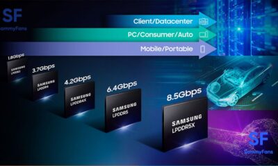
Samsung has completed industry-first validation of 16GB LPDDR6 on Qualcomm’s Snapdragon 8 Elite Extreme Gen 6 mobile platform. The memory has reached input/output speeds of up to 10.7Gbps and can deliver up to 114GB/s of bandwidth.
Additionally, Samsung says LPDDR6 improves power efficiency by up to 21% versus LPDDR5X through Dynamic Voltage and Frequency Scaling and Dynamic Efficiency Mode.
For Samsung, LPDDR6 could become a foundation for future Galaxy phones, although this validation does not confirm which upcoming models will adopt it.

SK Hynix LPDDR6
SK Hynix announced its 1c LPDDR6 development in March, reporting more than 10.7Gbps speeds and over 20% lower power consumption than LPDDR5X.
The company has planned mass-production preparations in the first half of 2026 and supply in the second half, targeting smartphones and tablets with on-device AI.
AI assistants are shifting from cloud-connected commands toward local processing of text, images, voice, and longer-running tasks. Those on-device AI workloads increase memory traffic while competing for battery power.







TSMC, Samsung, Intel, and SK Hynix are preparing to use a new technology, High-NA EUV, to make advanced computer chips. High-NA EUV is a powerful machine that can print very small designs on chips.
TSMC plans to use High-NA EUV for large-scale production of logic chips from 2030. Until then, it plans to continue using current EUV technology on its 2029 roadmap. This shows that TSMC is taking a careful approach to the new technology.
Samsung aims to use High-NA EUV earlier, starting with DRAM memory production in 2028. DRAM is a type of memory used in computers, smartphones and other electronic devices. SK Hynix is also expected to use the technology for DRAM around 2028, according to later reports.
Intel has already started using High-NA EUV. In July 2026, the company said it had begun production with the new machine. Intel is using it on some layers of its Panther Lake chips. However, the technology is still being used only on selected layers.

High-NA EUV machines are made by ASML. They have bigger mirrors than older EUV machines. This helps chipmakers print smaller designs and may reduce the number of steps needed to make some parts of a chip.
The companies are also looking at changing from 6-inch to 12-inch photomasks. Photomasks carry the chip design used during manufacturing. Bigger masks could help produce more chips in less time. However, announced dates are plans, and they do not always mean full production will begin exactly on those dates.

The fast growth of AI is increasing demand for computer memory. This has pushed DRAM prices to very high levels. A recent analysis says that the value of the latest DRAM memory is now higher per unit of area than the cost of producing advanced chips at TSMC.
According to the latest information, a 300mm wafer made using TSMC’s 3nm technology is estimated to cost about $20,000. That’s about $0.283 per square millimeter. A wafer made using the newer 2nm technology is estimated to cost about $30,000, or $0.424 per square millimeter.
The value of DRAM has increased as newer memory technologies provide more storage in the same area. Kernel Insights estimates that 1y DRAM is worth about $0.329 per square millimeter, while 1z DRAM is worth around $0.410.
The newest 1b DRAM is even more valuable. Its estimated value is about $0.654 per square millimeter. This is more than 50% higher than the estimated value of TSMC’s 2nm wafer area.
Strong DDR5 prices are also supporting this trend. DRAMeXchange recently reported an average price of $24.80 for a 16Gb DDR5 eTT chip, or about $1.55 per gigabit.
However, the comparison has some limits. TSMC’s figures are based on wafer processing, while DRAM figures represent the value of finished memory chips. Packaging and other costs are also different.
Even so, the figures show how strongly AI is increasing demand for memory. If DRAM prices stay high, memory companies could continue to see strong profits.


Samsung Electronics appears to be reshaping its roadmap for next-generation DRAM, with B1b technology now taking the lead in what was previously positioned as the company’s D0a generation.
ZDNet reports Samsung has moved B1b into its official DRAM roadmap and is using the D0a designation for this technology. The company’s earlier D0a concept, based on Vertical Channel Transistor (VCT) DRAM, is reportedly being separated as D0a-V.
B1b could bring sub-10nm DRAM sooner
The change reflects a practical shift in Samsung’s approach to scaling DRAM. B1b separates memory cells from their peripheral circuitry and manufactures them independently before connecting the two wafers through wafer-to-wafer hybrid bonding.
This architecture can improve density while allowing the cell and peripheral regions to use manufacturing processes better suited to their individual requirements.
Hybrid bonding also avoids conventional micro-bumps, potentially helping Samsung achieve tighter integration. B1b builds on hybrid-bonding techniques already used in other advanced semiconductor applications.
Samsung is reportedly considering B1b for HBM5, the next major generation of high-bandwidth memory, which is expected to arrive toward the end of the decade.
The first B1b-based D0a products could reach commercialization in roughly two years, although Samsung is expected to finalize major production investment plans later in 2027.

Samsung and SK Hynix are stepping up high-bandwidth memory (HBM) production as AI data centers continue driving demand for advanced memory.
Samsung prepares major HBM4 expansion
Samsung plans to raise average monthly HBM wafer input from around 180,000 units this year to approximately 250,000 in 2027, representing an increase of nearly 40%. HBM4 and HBM4E are expected to account for about 80% of Samsung’s HBM shipments next year.
The move follows improvements in Samsung’s HBM4 manufacturing process. Its reported yield has risen from below 60% during the early production phase to around 80%, allowing the company to produce more usable chips.
Counterpoint Research data shows its HBM revenue share increased from 21% in Q1 to 33% in Q2 2026, while SK hynix remained ahead at 50%.

SK Hynix also expands capacity
SK Hynix is accelerating its own production investments to maintain its position as AI memory demand grows. The company is expanding capacity at its M15X facility while advancing preparations for its Yongin semiconductor cluster.
The competition could become increasingly important as HBM4 adoption grows. More production from Samsung and SK hynix should help meet AI infrastructure demand.
If Samsung’s improved yields translate into reliable large-scale shipments, the company could further narrow the existing market-share gap with SK hynix while strengthening its role in the rapidly expanding AI memory market.
Samsung has started a major investment in Gwangju, South Korea, to support the semiconductor industry in the region. The company recently held a groundbreaking ceremony for a new heating, ventilation, and air conditioning (HVAC) production line at its Gwangju plant. These systems are important for semiconductor factories.
The Korean Tech giant will invest 240 billion won in the new facility. The company plans to complete the project and start operations in the first half of 2028. The facility is also expected to create around 300 new jobs.
This is Samsung’s biggest investment in Gwangju since the company opened its plant there in 1989. It is also the company’s first semiconductor-related investment in the Honam region. Samsung has also announced plans to build two semiconductor factories in Gwangju as part of its larger investment plans.
Meanwhile, Amkor Technology Korea is planning to expand its semiconductor packaging operations in Gwangju. The company plans to invest about 1 trillion won by 2035 and build six new production facilities.
A major wastewater issue related to Amkor’s expansion has also been solved. Gwangju City and Jangseong County plan to treat around 3,500 tons of wastewater produced every day by connecting the facilities to an existing wastewater treatment plant.
Together, these projects could help Gwangju develop a complete semiconductor industry. The region could bring together chip manufacturing, packaging, testing, equipment, materials, and research facilities.
Local officials also plan to improve important infrastructure, including electricity and water supplies, to support the growth of the semiconductor cluster.
-

 One UI3 days ago
Samsung Galaxy S23 gets One UI 9 Beta Hotfix with September 2026 patch
-
 One UI3 days ago
Global One UI 9.0 rollout begins for Galaxy S26 flagships in the US
-
 Samsung3 days ago
What could be the price of Galaxy S27 Ultra with 16GB LPDDR6 model?
-
 One UI1 day ago
One UI 9 stable update has these 14 new features, 5 changes, and 10 improvements