
Semiconductor
Samsung Exynos 2700 die shot gives first look at Galaxy S27 Ultra chip


Samsung is working on a new powerful smartphone processor, the Exynos 2700. The chip is expected to arrive in 2027 and could be used in Samsung’s future flagship phones.
A new die-shot of the Exynos 2700 has reportedly been shared by SemiAnalysis. A die-shot is basically a close look at the inside design of a chip. The image gives us an early idea of what Samsung’s next flagship processor may look like.
The Exynos 2700 is reportedly being made using Samsung’s SF2P process. It could have a 10-core CPU. The processor may include two powerful C2 Ultra cores and eight C2 Pro cores.
One of the Ultra cores could run at up to 4.24GHz, while the other may run at 3.36GHz. There could also be four C2 Pro cores running at 3.74GHz and four more running at 2.88GHz.
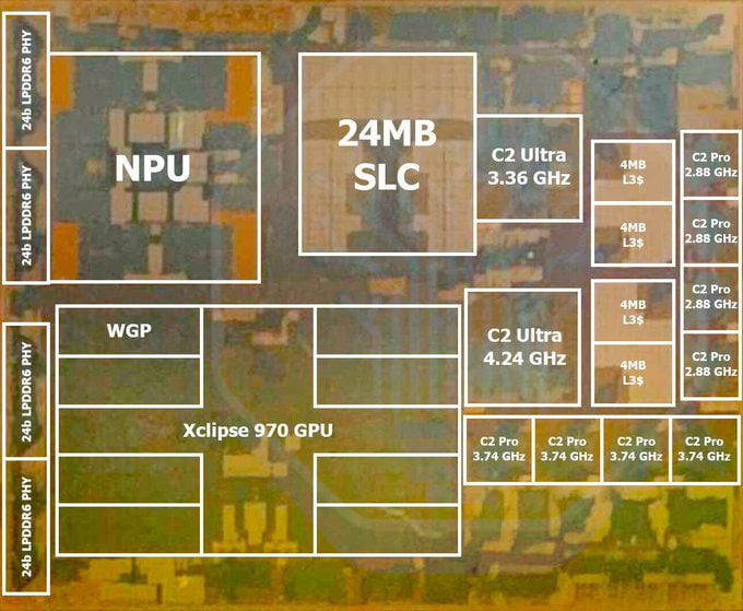
Image via SemiAnalysis
For gaming and graphics, Samsung is reportedly preparing the Xclipse 970 GPU. The Exynos 2700 may also include a dedicated NPU to improve AI features on smartphones. It support LPDDR6 memory, which could offer faster performance and better efficiency in future phones.
Samsung may use the Exynos 2700 in the Galaxy S27 Ultra in some countries. South Korea could be one of these markets, while countries such as the US may continue to get Snapdragon-powered models.
However, all these details are based on early reports and have not been officially confirmed by Samsung. More information should become available before the Exynos 2700 launches in 2027.





Samsung Electronics is taking its use of generative AI beyond software development, with the company testing Anthropic’s Claude in semiconductor design and verification work.
According to recent reports from South Korea, Samsung System LSI division has been using Claude Code to automate parts of custom system-on-chip (SoC) verification and early-stage semiconductor development.
After industry reports, CEO of Anthropic’s Korean subsidiary has now officially confirmed Samsung’s use of Claude Code in semiconductor design-related work.
In a recent interview with Maeil Business Newspaper at the Anthropic Korea office in Gangnam-gu, Seoul, Choi Ki-young, CEO of Anthropic Korea, stated, “Samsung Electronics is testing the application of Claude to semiconductor design tasks.”
CEO Choi added, “While Samsung researchers have handled specialized design software manually, there have been no instances of automating such design work using AI. This is an area where Claude is virtually the only one capable of handling it.”
Samsung’s AI chip design effort does not mean engineers are being removed from the process. Claude can generate verification environments, prepare test scenarios, and help identify potential issues, but its output still requires human review.
The company is also using other generative AI models, including Google Gemini and ChatGPT, as part of a wider AI transformation across its businesses.

Samsung just revealed its AI memory roadmap with ambitious performance targets for future products, including HBM5 and zHBM.
The company is laying out a much more ambitious roadmap for AI memory, with HBM5 positioned as the next major step before the company moves toward a fundamentally different 3D architecture.
At the Memory Executive Summit held alongside SEMICON Taiwan 2026, Samsung’s Choi Jang-seok outlined the company’s new “CUBE” strategy, which focuses on capacity, bandwidth, utilization, and power and thermal efficiency.
HBM5 aims for a major performance jump
HBM5 is expected to deliver roughly twice the performance of HBM4E, while improving performance per watt by 20% and reducing thermal resistance by another 20%.
Samsung has already shown an HBM5 mockup featuring its new Heat Path Block thermal-management technology; however, HBM5 is not the most interesting part of Samsung’s plan.
Samsung’s zHBM could change how AI memory is built
Samsung is reportedly looking beyond conventional HBM stacking with zHBM, which places HBM directly above the AI accelerator rather than alongside it.
The company expects a future interface using zHBM could reach up to eight times the performance of HBM5, while delivering up to three times better energy efficiency and cutting thermal resistance by more than half.
This makes Samsung’s zHBM more than a simple generational upgrade. The company is moving toward a memory architecture where reducing data movement becomes just as important as increasing bandwidth.
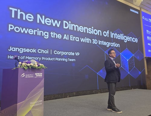
Image source – ET News

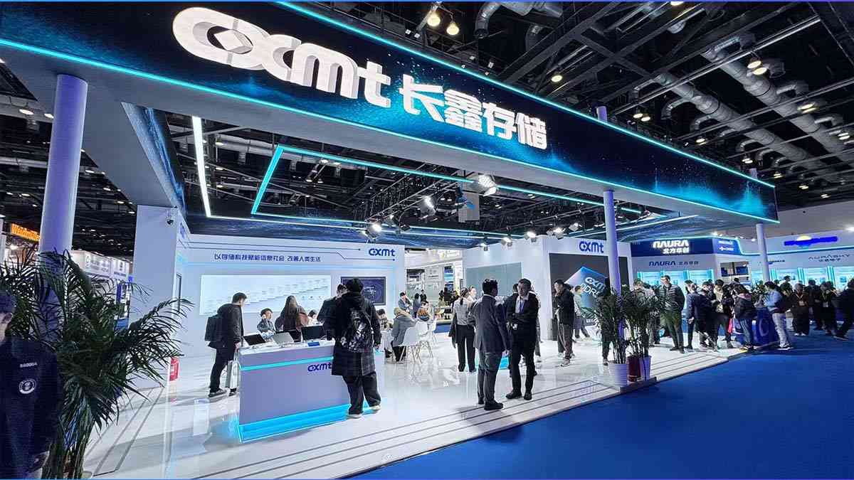
China’s memory ambitions are moving deeper into the AI hardware market. CXMT has reportedly started producing HBM3E in small quantities, giving Chinese chipmakers a local source for one of the most important components in AI chips.
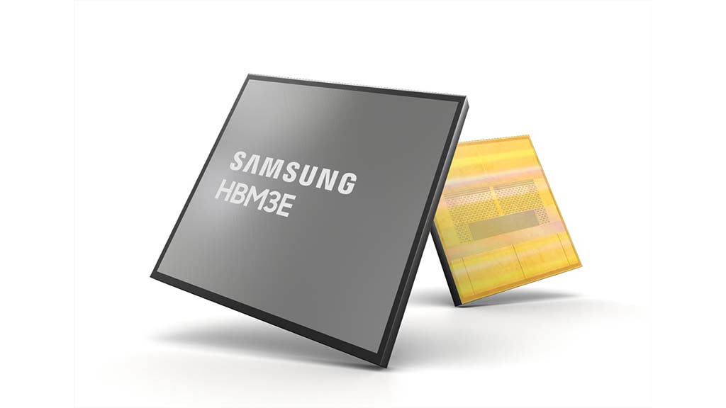
HBM3E is designed by stacking multiple DRAM dies and placing them close to an AI processor, providing the high bandwidth required for training and running AI models. CXMT is reportedly planning to expand production in 2027, reports TheInformation.
Chinese chip designers, including Alibaba’s T-Head and Cambricon, are already testing CXMT’s memory with their own processors. If qualification goes smoothly, products using the locally produced HBM3E could arrive as early as next year.
CXMT still trails Samsung and SK Hynix
The development is significant, but it does not mean CXMT has caught up with Samsung Electronics, SK Hynix, or Micron. The leading memory makers are already producing HBM4, while CXMT’s reported HBM3E production remains at a small scale.
CXMT is also facing challenges with yield, reliability, and manufacturing equipment. Reports indicate its HBM technology could still trail the leading players by several years.
Still, the progress could strengthen China’s domestic AI supply chain, particularly as U.S. export restrictions have made access to advanced HBM more difficult.
CXMT’s recent $8.6 billion IPO also gives it substantial funding to expand beyond conventional DRAM and compete in higher-value memory markets.
LG Electronics is working with CoAsia SEMI to develop two new chips for its AI-powered home products. The chips will be made by Samsung Electronics’ semiconductor manufacturing business.
CoAsia SEMI announced the project on August 31. It is part of South Korea’s government-supported “K-On-Device AI Semiconductor Technology Development” project. The project will continue until December 2030, with a total development cost of about 31 billion won.
LG will decide what the chips should do and provide the required specifications. CoAsia SEMI will design the chips and make sure they can be produced using Samsung’s manufacturing technology. Employees from CoAsia NEXELL, another company in the CoAsia Group, may also help with the work.
The new chips will be used in AI home products and IoT devices. IoT means connected devices that can collect and share information. The companies want to make the chips use very little electricity while allowing home devices to continuously sense and understand their surroundings.
The decision is important because LG Electronics has mainly used TSMC to manufacture chips for its home appliances. Choosing Samsung Foundry is therefore unusual for LG.
The Korean government’s AI semiconductor project aims to develop advanced chips for many industries, including cars, home appliances, robots, machinery, defense and IoT devices. The program has a budget of about 800 billion won and will run until 2030.
CoAsia SEMI CEO Shin Dong-soo said the company hopes its partnership with LG will create more business opportunities in AI home products and other markets.
SK Hynix CEO Kwak Noh-jung believes the shortage of memory chips could continue until the end of 2030. He said he does not see any clear signs of too many memory chips in the market.
Kwak shared his views after SK Hynix started work on a new chip packaging plant in Indiana, USA. The company is investing in the United States because demand for advanced memory chips is growing quickly.
A major reason for this demand is AI. Companies are spending huge amounts of money to build AI data centers and powerful computers. These systems need large amounts of advanced memory, mainly HBM.
Kwak said memory chips are no longer just basic products. In the past, memory companies mainly made standard chips, which often led to periods of oversupply and falling prices. AI is now changing this situation. Many new memory products are being designed for specific customers and their needs.
Kwak believes this could make future market downturns different from those in the past. He also does not expect AI-related memory demand to suddenly disappear after 2030.
SK Hynix is one of Nvidia’s important memory suppliers. Nvidia has secured about $279 billion in supply and expects its business to grow around 70% through fiscal 2028. Kwak also said SK Hynix could make more investments in the U.S. if there is enough electricity, money and government support. However, investors should remain careful.
-
 One UI3 days ago
Samsung’s August 2026 update released for Galaxy S23, S24, S25, S26, FE, foldables and more
-
 Updates2 days ago
Samsung releases August 2026 update in more regions for Galaxy S26, S25, S24, and more
-

 One UI1 day ago
Samsung releases One UI 9.0 Beta for Galaxy S25 series and S25 FE; join and download Beta 1 now
-

 Updates2 days ago
Samsung updates Galaxy A57, A56 and M56 with August 2026 security patch