News
Samsung gets Life Cycle Assessment verification on product carbon footprint of semiconductor
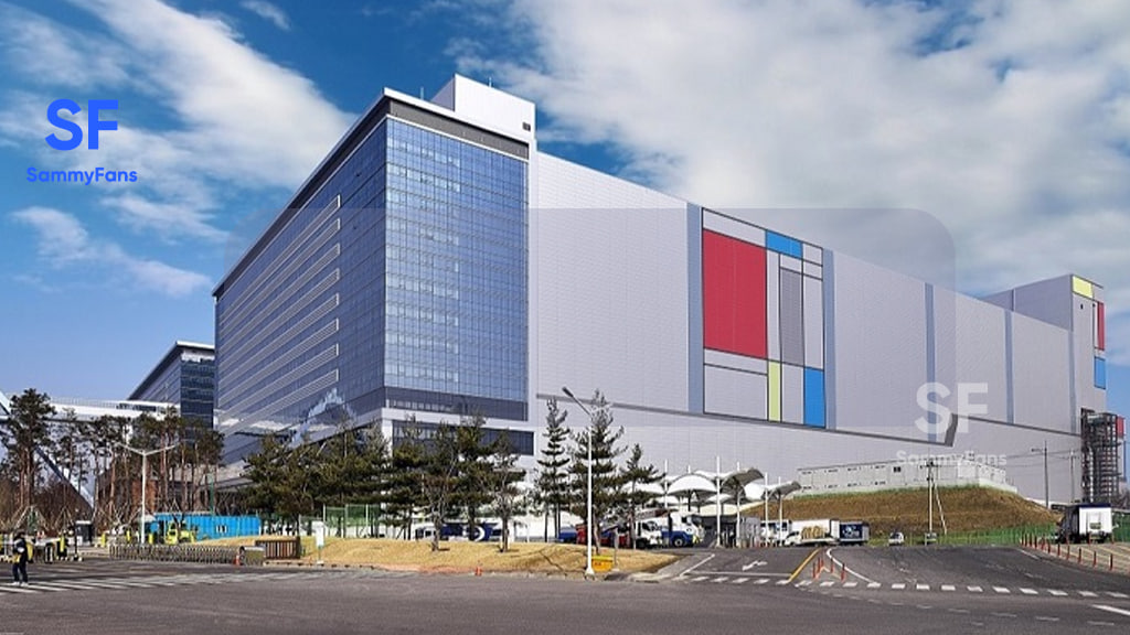
Samsung has established a credible Life Cycle Assessment (LCA) to create a more sustainable environment in the future by achieving carbon neutrality. The purpose of developing LCA is to get the product carbon footprint of its semiconductor business.
Join Sammy Fans on Telegram
One of the world’s leading independent certification bodies, DNV has verified LCA establishments to take part in overcoming the climate crisis and achieving carbon neutrality.
Follow Sammy Fans on Google News
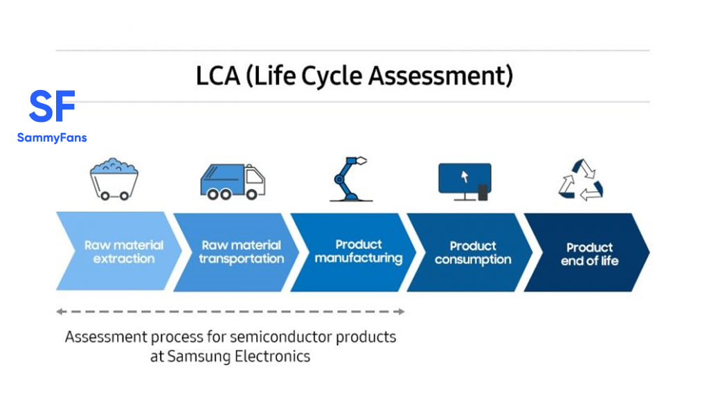
LCA is an approach for assessing the environmental impact of a commercial product, process, and service throughout its life cycle by quantifying energy, material, and waste emissions. Specifically, on the carbon footprint of semiconductors, Samsung’s LCA covers the extraction of raw materials for chip manufacturing, assembly, and testing. Its calculation is based on ISO 14040, ISO 14044, and ISO 14067 to ensure reliability and transparency.
Samsung and its customers commonly use the Carbon Footprint to identify the environmental impact of all stages of Samsung’s semiconductor products and can be used as an indicator to track and reduce carbon emissions.
So far, 37 of Samsung’s semiconductor products including DRAM, SSD, embedded storage, mobile SoC, mobile Image Sensor, and automotive LED packages have received Carbon Trust and UL’s Carbon Footprint certification. In addition to this, 6 memory products have received Carbon Trust’s Carbon Emission certification.
Using LCA established late last year, Samsung will measure the carbon footprint of chips produced at all of its global manufacturing, testing, and assembly sites in South Korea, China, and the United States.
Samsung will expand its Life Cycle Assessment to include water and resource footprints to provide a more comprehensive assessment that will eventually reduce the application’s effect on the environment.
According to Dooguen Song, Executive Vice President of the Environment, Health and Safety (EHS) Center at Samsung Electronics:
“Since 2019, we have been actively mobilizing efforts to measure and reduce the carbon emissions of our key memory and logic solutions. By leveraging LCA, we will be able to support our customers to achieve their carbon neutrality, as well as becoming more transparent on the environmental impact of the semiconductors we produce worldwide.”


Samsung’s executive chairman Jay Y. Lee (Lee Jae-yong in Korean) topped the Forbes 2024 Richest Korean list for the first time. On April 17, Forbes revealed that the Samsung boss is the richest in South Korea, with his assets increasing by $3.5 billion, bringing his total net worth to $11.5 billion.
Thanks to a rise in Samsung’s stocks, Samsung’s Lee jumped to the top of the Forbes 2024 Richest Korean list. Notably, the company’s stocks significantly hiked after the revelation that it’s developing high-bandwidth memory chips used in AI computing for NVIDIA.
Forbes 2023 Richest Korean, Kim Byung-ju, slipped to second this year with assets worth $9.7 billion. The third place went to Seo Jung-jin, honorary chairman of Celltrion, with assets of $7.5 billion.
Cho Jung-ho, chairman of Meritz Financial Group, ranked fourth with $6.2 billion, and Chung Mong-koo, honorary chairman of Hyundai Motor Group, was fifth with $4.6 billion.

Stay up-to-date on Samsung Galaxy, One UI & Tech Stuffs by following Sammy Fans on X/Twitter. You can also discover the latest news, polls, reviews, and new features for Samsung & Google Apps, Galaxy Phones, and the One UI/Android operating system.
Do you like this post? Kindly, let us know on X/Twitter: we love hearing your feedback! If you prefer using other social platforms besides X, follow/join us on Google News, Facebook, and Telegram.
Samsung established an AI chip design-dedicated Advanced Processor Lab in Silicon Valley, US. Formerly known as the Advanced Institute of Technology, Samsung’s SAIT is said to have formed the new Lab to strengthen its AI chip R&D in the US.
BusinessKorea reports that the new Samsung Advanced Processor Lab to focus on developing next-gen AI semiconductor design assets in the US. The assets are said to be focused on the RISC-V area, which serves as a foundational design asset for semiconductor chip design.
Samsung’s initiative with RISC-V is interpreted as a move towards technological independence. Therefore, the company is expanding its R&D organization in Silicon Valley, aiming to enhance design capabilities to disrupt the market currently dominated by NVIDIA.
Amid the booming AI era, the market of advanced semiconductors is also expanding. Samsung has completed the development of its Mach-1 AI semiconductor and supplied prototypes to global firms including Korea’s Naver. The company has also started the development of Mach-2.
Under the CHIPS Act, Samsung received huge subsidies to boost investment in the US. It’s worth noting that the Biden govt awarded a 12% subsidy of Samsung’s total investment, which is significantly higher than Intel and TSMC’s subsidy.
Stay up-to-date on Samsung Galaxy, One UI & Tech Stuffs by following Sammy Fans on X/Twitter. You can also discover the latest news, polls, reviews, and new features for Samsung & Google Apps, Galaxy Phones, and the One UI/Android operating system.
Do you like this post? Kindly, let us know on X/Twitter: we love hearing your feedback! If you prefer using other social platforms besides X, follow/join us on Google News, Facebook, and Telegram.

Samsung’s first 3nm Exynos 2500 chip could outpace Snapdragon 8 Gen 4 in power efficiency. Both chipsets will power the next-gen Galaxy flagships, scheduled for an early 2025 launch. Recent input suggests that Exynos is returning as a tough rival to Snapdragon.
The Exynos 2500 will be made on Samsung’s 2nd-gen 3nm process technology. The S24’s Exynos 2400 chipset impressed the industry with significant improvements over its predecessor. The company appears to be leveling up the game next year.
Thanks to the cutting-edge process node, Samsung’s next Exynos could finally surpass its Snapdragon counterpart in power efficiency. The company may utilize its advanced FOWLP in the Exynos 2500 to make it run at higher clock speeds at the same power consumption level.
Qualcomm is facing power efficiency concerns with its recent Snapdragon chips. Due to reduced efficiency, phone makers are forced to bring up to 5000mAh battery. Samsung apparently seized this opportunity to bring back its in-house Exynos back to the contest.
Stay up-to-date on Samsung Galaxy, One UI & Tech Stuffs by following Sammy Fans on X/Twitter. You can also discover the latest news, polls, reviews, and new features for Samsung & Google Apps, Galaxy Phones, and the One UI/Android operating system.
Do you like this post? Kindly, let us know on X/Twitter: we love hearing your feedback! If you prefer using other social platforms besides X, follow/join us on Google News, Facebook, and Telegram.