News
Samsung is looking to develop 1.4nm semiconductor chips by 2027

Today, at the annual Samsung Foundry Forum event, the company has officially unveiled its plans for Foundry Business with the introduction of cutting-edge technologies. Samsung is planning to manufacture 2nm process technology by 2025 and 1.4nm semiconductor chips by 2027.
Samsung is the world’s second-biggest semiconductor chip manufacturing firm. The company reveals that the demand for advanced semiconductors has increased dramatically and that’s because of the significant market growth in high-performance computing (HPC), artificial intelligence (AI), 5G/6G connectivity, and automotive applications.
Join SammyFans on Telegram
Therefore, Samsung emphasized its promise to bring its most advanced process technology, 1.4nm semiconductor chips for mass production in 2027.
Follow Sammy Fans on Google News
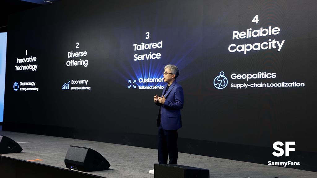

In addition to this, the Korean company has also highlighted the steps its Foundry Business is taking in order to meet customers’ needs. These include:
- Foundry process technology innovation
- Process technology optimization for each specific applications
- Stable production capabilities
- Customized services for customers
President and head of Samsung Foundry Business said that technology development targets of up to 1.4nm and specialized foundry platforms for each application, along with stable supply through continued investments, are part of Samsung’s strategies to secure customer trust and support their success.
Samsung 1.4nm Advanced Node Roadmap:
Samsung gains huge success with the latest 3nm process technology. With this, the company plans to further enhance the Get-All-Around (GAA) based technology and schedules to launch a 2nm process in 2025 and a 1.4nm process in 2027.
In the meantime, the company is also gearing up the development of 2.5D/3D heterogeneous integration packaging technology to provide a total system solution in foundry services.
According to the information, Samsung’s 3D packaging X-Cube with micro-bump interconnection will be ready for mass production in 2024, and bump-less X-Cube will be available in 2026.


Furthermore, the company has also unveiled that it is planning to expand its production capacity for the advanced nodes by more than three times by 2027 compared to this year. At the event, it detailed the “Shell-First” strategy for capacity investment to better respond to customers’ demands.
Lastly, Samsung said that it will hold the ‘SAFE Forum’ (Samsung Advanced Foundry Ecosystem) on October 4th. At that event, it will introduce foundry technologies and strategies with ecosystem partners such as Electronic Design Automation (EDA), IP, Outsourced Semiconductor Assembly and Test (OSAT), Design Solution Partner (DSP), and the Cloud.
For more information, visit Samsung Newsroom.