News
Samsung investing $15 billion to build advanced research facility

Today, Samsung has established a new semiconductor R&D (Research and Development) complex in Giheung, South Korea. With this, Samsung building an advanced research facility that aims to extend its leadership in state-of-the-art semiconductor technology.
Download Sammy Fans App
Samsung said it is planning to invest about KRW 20 trillion (~ USD 15 billion) by 2028 for this complex in an area of about 109,000 square meters within its Giheung campus.
This new establishment will conduct advanced research on next-generation devices and processes for memory and system semiconductors, as well as the development of innovative new technologies based on a long-term roadmap.
Join SammyFans on Telegram
Samsung is looking to overcome the limits of semiconductor scaling and solidify its competitive edge in semiconductor technology, with the establishment of this advanced research facility.
Follow Sammy Fans on Google News

Samsung’s new Giheung R&D structure, along with an R&D line in Hwaseong and the world’s largest semiconductor production complex in Pyeongtaek, is also expected to enhance synergy between Samsung’s three main semiconductor campuses in the urban region.
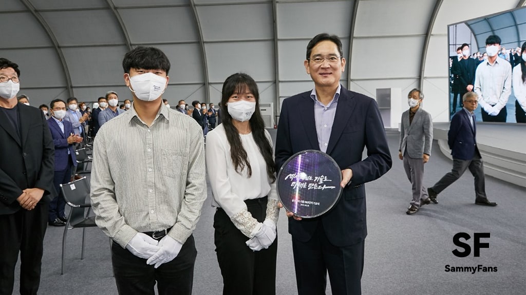
Further, this establishment ceremony was attended by Samsung Electronics Vice Chairman Jay Y. Lee, President and CEO Kye Hyun Kyung, President of the Memory Business Jung-Bae Lee, President of the Foundry Business Siyoung Choi and President of the S.LSI Business Yong-In Park, along with more than 100 employees.
Samsung’s Giheung campus, located south of Seoul near the DS division’s Hwaseong campus, is the birthplace of the world’s first 64MB of DRAM in 1992, marking the beginning of the company’s semiconductor leadership.
For more information, visit Samsung Newsroom.