News
Sony developed world’s first stacked CMOS image sensor technology

Sony is one of the world’s largest makers of CMOS image sensors, as its chips are widely used in digital cameras, tablet computers, smartphones, drones, and most recently, self-driving systems such as automobiles, along with Samsung and Omnivision.
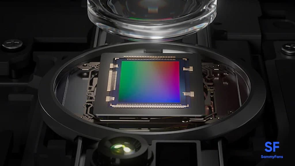
Sony company is generally at the cutting edge of smartphone photography and has announced another great innovation in space. Recently, the Japanese company announced its the world’s first stacked CMOS image sensor with a “2-layer transistor pixel”. So what does this really mean?
Sony also posted a picture to give people a better idea of what has changed compared to traditional censorship. You can see this picture below.


Sony doubles the saturated signal level of this solution sensor and thus offers a wider dynamic range. The company claims that moving pixel transistors to a different substrate can free up space to increase the size of so-called amp transistors.
This suggests that larger amp transistors produce less noise, which is advantageous for low-light photography. This technology allows the pixels of the sensor to maintain or enhance their current performance even at small pixel sizes.

Particularly, Sony seems to think that this technology will be crucial for high-resolution smartphone cameras with smaller pixels. So if the company wants to offer 108MP or 200MP cameras following in Samsung’s footsteps so it will be an important enabler.
Sony has assured that the technology is for smartphones, but has not given a timeline for when to look at the first sensors with this layout. However, it is still fascinating that camera sensor manufacturers are constantly making innovations in this area.
//Source